Once upon a time, ASIC designers were integrating memories in their design (using a memory compiler being part of the design tools provided by the ASIC vendor), then they had to make the memory observable, controllable… and start developing the test program for the function, not a very enthusiastic task (“AAAA” and “5555” and other vectors), look for the test coverage, and try to be creative to reach the expected 99,99% magic number. I agree that this was long time ago, but when looking back to this old time, you realize how powerful is DesignWare Self-Test and Repair (STAR) Memory System from Synopsys, initially developed by Virage Logic. Today we are talking about the version 5 of the tool. Moreover, since the year 2000’s, most of the ASIC vendors are externally sourcing the SRAM compiler (to Virage Logic at that time…), ASIC designer is taking benefit of faster, denser memories with Built-In-Self-Test (BIST) integrated.
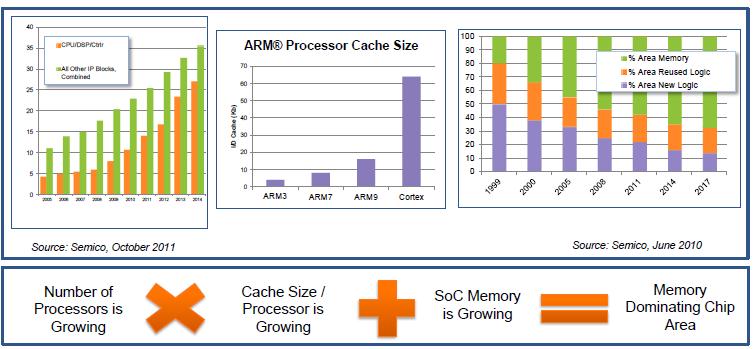
According with Semico, the number of processors integrated into a single SoC is growing (left caption, even if I am not sure that 16 processor per SoC is the standard in 2012 for every SoC, this is certainly the case with Application Processor for smartphone or Set-Top-Box), and, as a matter of fact, processor cache size is growing (middle caption), leading memory to dominate chip area, as we can see on the right of the picture. Leading to an immediate consequence on the SoC yield: it would dramatically decrease, if… the designer don’t use repair capability, like for example this offered by the STAR product (for Self-Test and Repair). Another precision about STAR version 5: unlike the previous version sold by Virage Logic, the tool can be available for a memory generated by a compiler coming from any vendor. Last, but not least precision, STAR Memory System 5 is targeted for designs implemented at 20-nm and below technologies.
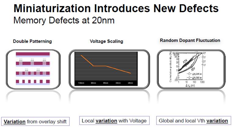
You may want to challenge the assertion claiming that SoC yield would be severely impacted when integrating higher SRAM proportion within IC at 20nm and below? Thus, just have a look at the above pictures:
- Double patterning introduces variation from overlay shift,
- Voltage Scaling induces local variation with voltage, and
- Random Dopant Fluctuation generates global and local Vth variation
These process variations become significant at 20nm, causing bit failure. Implementing SRAM in a system (on Chip) is no more a “drag and drop” action, the designer has to also take into account a solid (automated) test generation, as well as to introduce repair capability, as the risk of failure is statistically… a certitude.
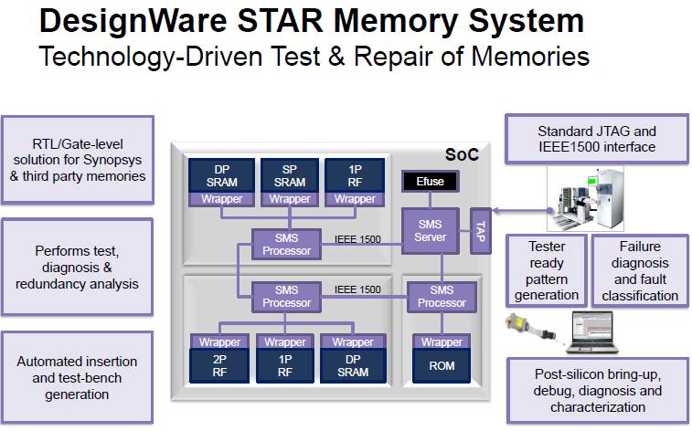
STAR Memory System 5 can be implemented for SRAM, as already mentioned, and also for ROM, Register File or Content Addressable Memory (CAM). The designer will implement a specific wrapper interfacing with the various memories, and a real memory sub-system is created, comprising a master and several slaves. The master, SMS Server, is connected to the outside world by a Test Access Port (TAP), and to several slaves (SMS Processors) through an IEEE 1500 normalized Bus. Each of the SMS Processors is connected to various memories (can be Single or Dual Port SRAM or Register Files) through the wrappers. Indeed, the test bench generation and the above described insertion are completely automated by STAR Memory System 5, also allowing performing diagnosis and redundancy analysis.
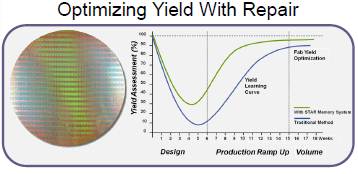
After running the test program on processed wafers, the failure diagnosis and fault classification will allow implementing redundancy, thanks to the Efuse box (Top right of the SoC block diagram), and dramatically increase the final SoC yield, as we can see per the image below.
To summarize, we have listed some unique features of the DesignWare STAR Memory System 5:
- Performance and area optimized architecture to efficiently test & repair thousands of memories with smaller area and less routing congestion
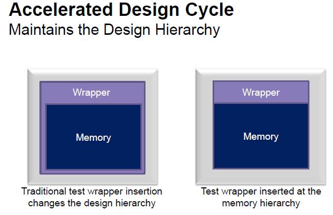
- Automated IP creation, hierarchical SoC insertion, integration, verification and tester-ready pattern generation
- Hardened STAR Memory System IP with Synopsys’ DesignWare memories enabling faster design closure, higher performance, higher ATPG coverage, smaller area and reduced power.
- Advanced failure analysis with logical/physical failed bitmaps, XY coordinates of failing bit cells and fault classification
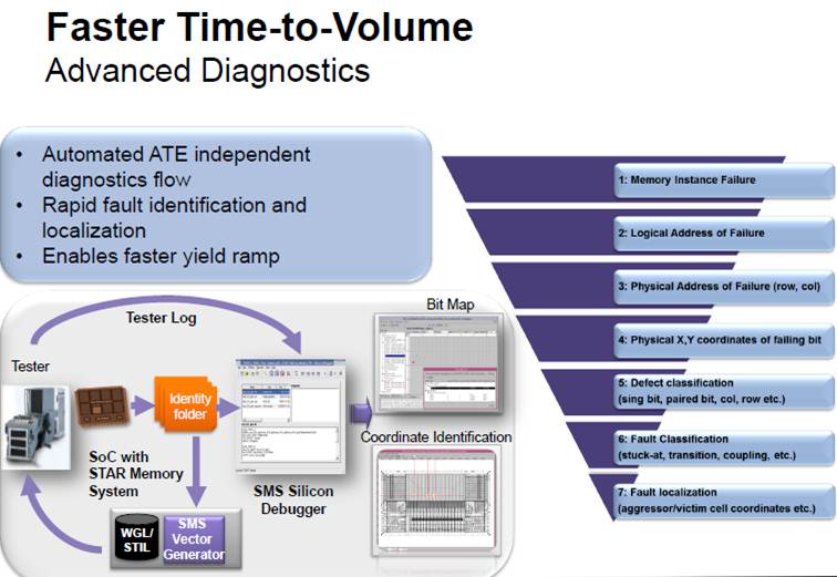
Important to notice, this new version offers:
- New optimized memory test and repair algorithms to efficiently address memory defects, including process variation faults and resistive faults, at 20-nm and below
- New hierarchical architecture reducing test & repair area by 30% compared with the previous generation
- Hierarchical implementation and validation accelerating design cycles by allowing incremental generation, integration and verification of test and repair IP at various design hierarchy
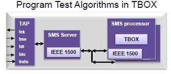
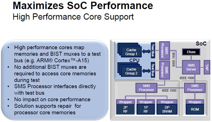
- Support for test interfaces of high-performance processor cores maximizes design productivity and SoC performance, see below:
You may want to read the official Press Release from Synopsys about STAR Memory System 5
Share this post via:


Comments
0 Replies to “How much SRAM proportion could be integrated in SoC at 20 nm and below?”
You must register or log in to view/post comments.