

Electronic Design and Solutions Fair (EDSF) was held in Yokohama Japan from Wednesday to Friday last week. It was held at the Pacifico Hotel, somewhere I have stayed several times, not far from the Yokohama branch of Hard Rock Cafe and, what used to be at least, the biggest ferris-wheel in the world.
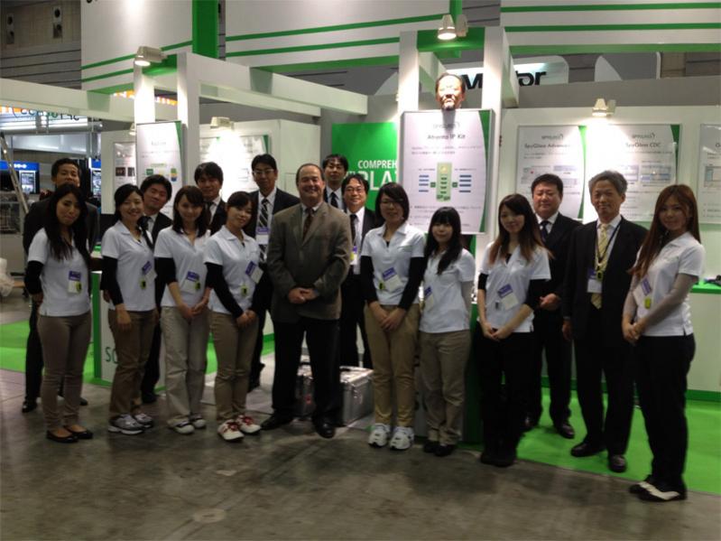
Atrenta was one of the many companies at EDSF2012. The EDS fair consists, for the second year, of a combination of what used to be a pure EDA show and the larger embedded show. Since Japan tends to be in the forefront of systems thinking, with Europe coming next and the US bringing up the rear, this combination is good since it brings in people from across the whole spectrum of design, not just a succession of CAD managers from the usual suspects. This is especially important for Atrenta since they are focused on doing design at a higher level with IP and software IP combined together to form systems.
Atrenta managed to generate a good supply of high-quality leads, each qualified by either an AE or a salesperson (so this doesn’t include students, press etc). Just like SemiWiki, students, press, PR and everyone are all very welcome but in the end it is the real design and embedded engineers who are the most important audience.
One thing that worked very well was the use of iPads as a way for customers to receive a deeper understanding of Atrenta’s products. They ported product presentation pdfs onto 8 iPads. In addition to salespeople and AEs using them as a tool to explain Atrenta’s products, the iPads also provided a venue for customers to get a deeper understanding of their products than they would typically receive from perusing a panel. It proved to be very effective as it allowed them to engaged with more customers than by using demos alone.
In terms of product interest, the highest was with BugScope. We believe this to be a combination of existing customers wanting to know about our newest product as well as designers looking for solutions to their verification challenges. Following closely behind where: SpyGlass CDC, SpyGlass for FPGA (we had a presentation highlighting SpyGlass plus CDC combined with the Xilinx Vivado support), and SpyGlass Power.
Meanwhile, back on this side of the Pacific, Ed Sperling had one of his round tables on the challenges of 3D, new process nodes. Venki Venkatesh of Atrenta was one of the participants. I’ve participated myself in a couple of Ed’s round tables. Basically he records the whole thing and then transcribes it (himself, it is so technical you can’t just give it to a secretary-type), cleans up the ums and ers and publishes it pretty much verbatim. You can find this one here. One of themes, as I’ve been pointing out, is that people are going to stay on 28nm as long as possible, that there is no rush to 20nm since the costs are a challenge (never mind the technical challenges).
There is also a short video version with the same people around the table here.


TSMC CoWoS versus Intel EMIB Semiconductor Packaging