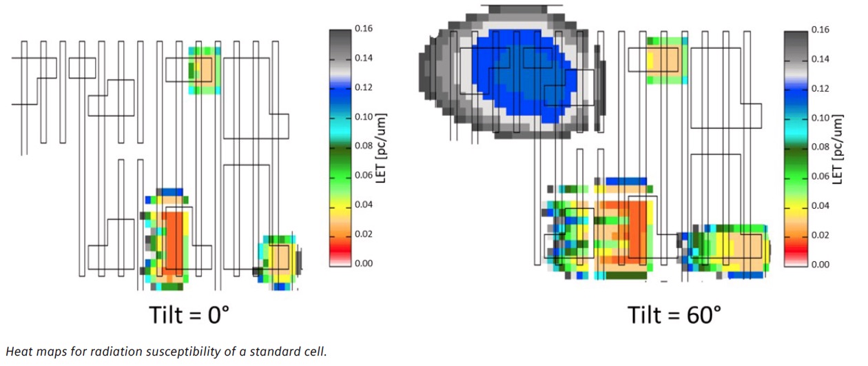
Much of the technology that goes into aerospace applications is some of the most advanced technology that exists. However, these same systems must also offer the highest level of reliability in what is arguably an extremely difficult environment. For semiconductors a major environmental risk in aerospace applications are the effects of charged particles in the upper atmosphere and space. Charged particles can lead to soft errors, where an IC is not permanently damaged, but its operation is temporarily disrupted leading to unpredictable results. Of course, ICs used in aerospace are hardened to limit the effects of charged particles, but their underlying process technology plays a big role in their susceptibility, especially in the case of FinFETs.

To lower the risk from charged particles, aerospace ICs have tended to use trailing process nodes. However, new nodes offer many attractive characteristics, such as reduced power and higher levels of integration. According to a Siemens EDA white paper, the European Space Agency (ESA) was interested in evaluating various FinFET nodes to determine which ones were the most promising candidates for use in their flight systems. The white paper titled “IROC tapes out aerospace SoC with Aprisa place-and-route” talks about ESA’s work with IROC Technologies to design test chips for evaluating the effects of charged particles on these advanced nodes.
IROC has broad capabilities for designing and testing ICs for quality and reliability. Yet, when ESA approached them to design self-contained test vehicles for FinFET processes they needed to put in place a complete FinFET SOC design flow for 16nm. The test chip design calls for standard cells, memories, complex IP and more. Along with the structures being tested the chip also had to include support circuitry to measure, record and analyze the performance of the test structures. The monitoring blocks had to be completely immune to radiation.
Like many companies looking for tools to set up their flow, IROC started looking at the tools qualified for the targeted TSMC N16 FinFET process. They were of course familiar with Calibre, but also saw that Siemens’ Aprisa place and route solution was included as well. IROC decided to proceed with using Aprisa for this project. Their initial decision, guided by Aprisa’s integration with other Siemens tools and tools from other vendors, was affirmed once they saw how intuitive and easy Aprisa was to set up and use. IROC used the reference flow provided by the Aprisa support team to go through their rapid learning process. One example of this smooth bring-up was the ease of setting up Aprisa to use the TSMC PDK for their process.
IROC started with the design partitioning step using a combination of custom and RTL based blocks. Aprisa let them generate the Liberty and layout views necessary for floor planning and chip assembly. Within a few days of setting up the flow they had completed first pass placement. The built-in timing analysis engine only required a few lines of Tcl to give them timing feedback that correlated well with their final sign off tools.
In the white paper IROC said they were pleased with the quick turnaround of the detail-route-centric design results provided by Aprisa’s multithreading capability. According to the white paper IROC saw high quality results that reduced the need for iterations to achieve design closure. In only three months IROC went from tool installation all the way through to a successful tapeout. For a FinFET process this is a remarkable achievement. They were able to use the silicon to perform the targeted reliability analysis for ESA. The aggressive schedule for the project meant that IROC made the decision to proceed with Aprisa without a traditional evaluation. Their assessment that the Aprisa would perform well for their project appears to have been well founded. No doubt the reputation that Siemens has earned for its EDA tools played a large factor in this decision. Aprisa is also certified down to TSMC N6 and is in the process of gaining certification for TSMC N5 and N4. The white paper is available for download on the Siemens EDA website.
Also read:
Path Based UPF Strategies Explained
Co-Developing IP and SoC Bring Up Firmware with PSS
Balancing Test Requirements with SOC Security
Share this post via:


Comments
2 Replies to “Designing a FinFET Test Chip for Radiation Threats”
You must register or log in to view/post comments.