The topic of Product Lifecycle Management (PLM) conjures up images of usage on airplanes, tanks and cars. That’s because it was developed decades ago to help make product development and delivery more efficient for big expensive manufactured products. It worked well for its intended markets by combining and managing all the phases of product development, parts procurement and manufacture. Unfortunately, while the concept is sound, there has been little feasible success implementing classic PLM systems for IC design.
There are several significant reasons that PLM has not gained traction in the IC design space. Traditionally PLM systems are applied by taking a relatively static design and manufacturing process and building an extensive set of customizations and specially tailored code to handle that one specific case. As we know IC design is changing at every node, and even at existing nodes, flows and tools always being updated. As a result, rather than setting up a system and using it continuously, IC design requires adaptability in PLM systems.
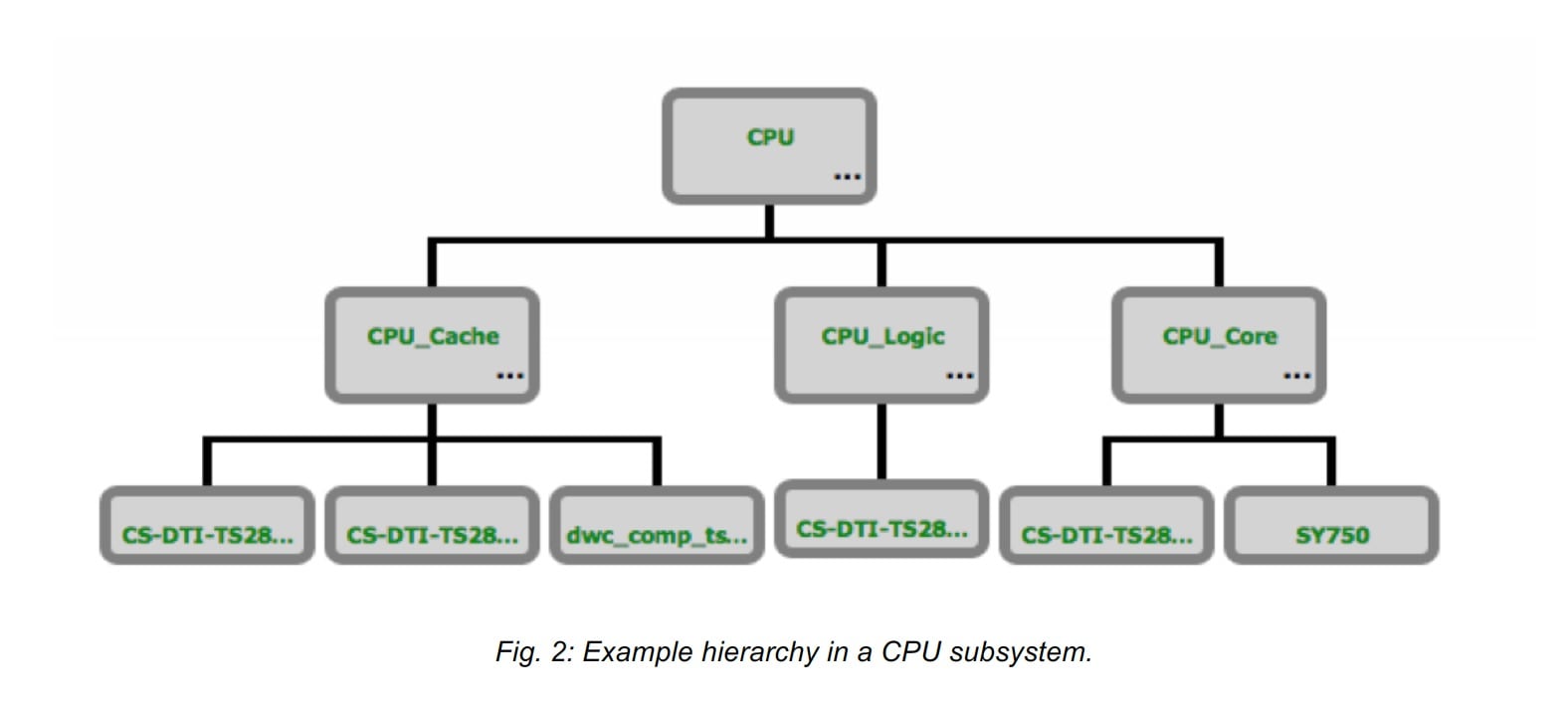
Another big difference in IC design is how semiconductor IP’s are really hierarchically self contained designs themselves. So rather than taking a flat bill of materials from suppliers or internal sources and assembling them in to a finished product, IC’s have layer upon layer of blocks that are each themselves potentially composed of smaller IP blocks. The requirement for semiconductor PLM’s is to manage all the design and verification steps at each level as information is moved from development to utilization.
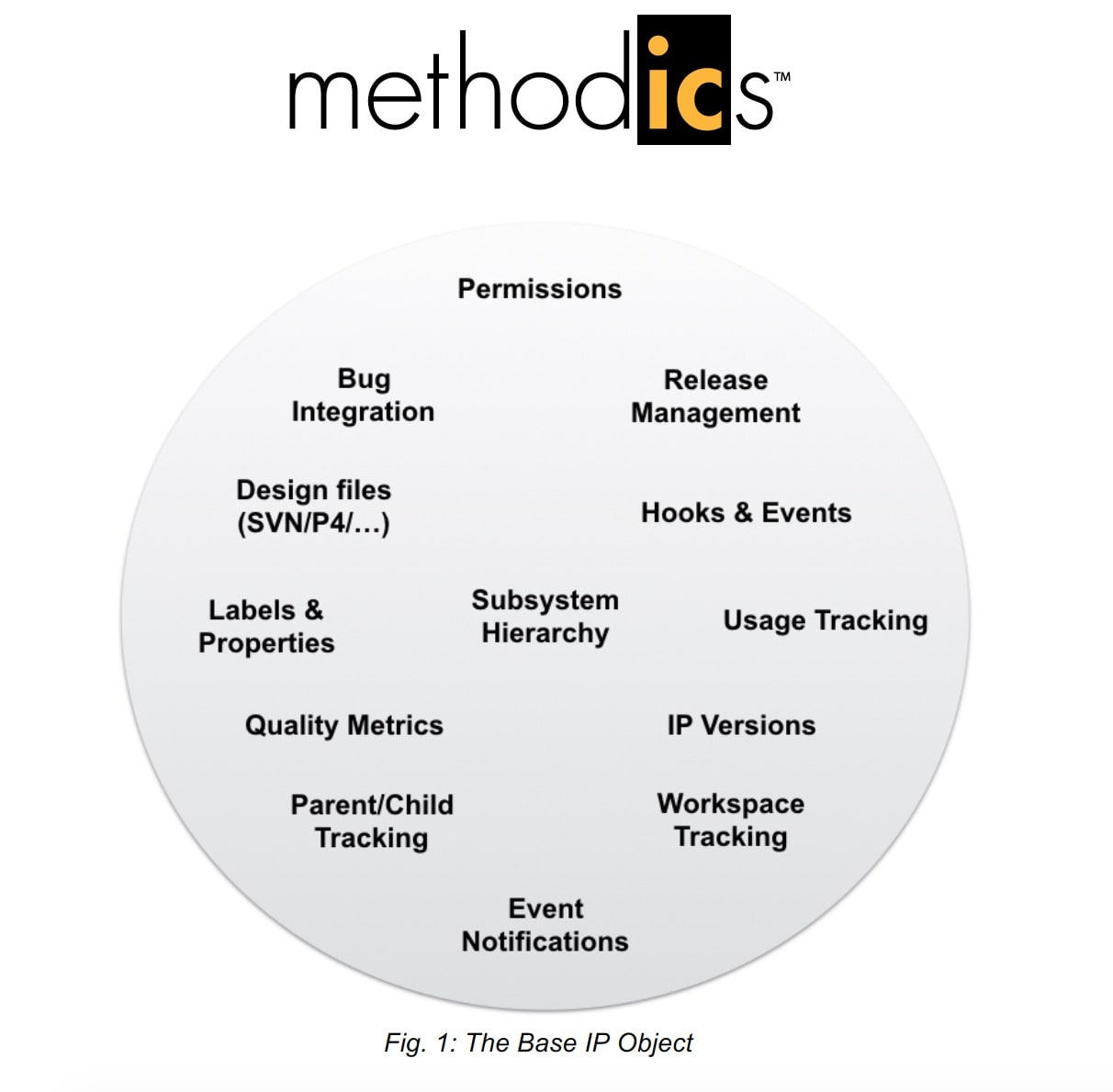
The data we are talking about includes technology files, tool versions, quality metrics, constraints specifications, dependencies, etc. Also access control and release management, and a number of other features are necessary. In fact, Methodics has compiled a list of all the properties that are needed in each base object in an IP PLM system.

Methodics is well versed on this topic because they have developed a PLM system specifically tailored to semiconductor design. It uses their ProjectIC design management system as its foundation. In turn ProjectIC is built upon industry standard revision control systems such as Perforce, GIT or Subersion, used in their native form. The real question, however, is what are the steps to connect Methodics’ IP Lifecycle Management (IPLM) system to a semiconductor design project and all of its potentially hierarchical IP components.

Fortunately, Methodics has written up a white paper that covers the fundamentals and also the integration points for their IPLM system. The process starts with customers adding in meta data for the IP that they wish to include. This can be run as a batch operation once the specific fields desired have been defined. There is some discretion here as to what to include, but the flexibility allows customers to attach whatever metadata they deem important for each IP block. It is also easy to update or modify these definitions.
Next is the process of importing existing IP into workspaces so they can be worked on and released to other users and teams. Now, IP can be changed and worked on in a systematic fashion. Also any tool run results can be captured and saved. This might include P&R results, or the output from verification runs such as DRC, simulation, etc. All this information is maintained with the IP for future reference and use.
At this point it is possible using Methodics’ IPLM system to create releases for the IP users who depend on the IP. As downstream users integrate these IP releases into their own designs, data about where the IP is used is saved. This means that it is possible to determine where specific IP is used.
Other metadata can be added back into the IPLM system from downstream users and external sources. Custom metadata can be created using the ProjectIC API’s. These comprehensive API’s are well documented and make it easy to create custom scripts to provide richer data on IP implementation and deployment within an enterprise.
The Methodics white paper goes into much deeper detail than we have space for here. If you are interested in how PLM can realistically be applied to semiconductor design, reading it is highly recommended. A copy is available through their website.
Share this post via:


Comments
There are no comments yet.
You must register or log in to view/post comments.