Semiconductor designs have been progressing over time to address wider product varieties and designs with increasing complexity. Organizations have been addressing intense time-to-market pressures by leveraging globally dispersed team resources. The project-centric design methodology, which once worked well with … Read More

Tag: methodics
IP Lifecycle Management for Chiplet-Based SoCs
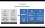
Chiplet-based System-on-Chips (SoCs) are becoming increasingly popular in the semiconductor industry due to their potential to improve design efficiency, increase performance, and reduce costs. While chiplets are seen as a way to reduce the cost of innovation, they introduce a lot of challenges too. Packaging, interconnect… Read More
Podcast EP132: The Growing Footprint of Methodics IPLM with Simon Butler
Dan is joined by Simon Butler, the founder and CEO of Methodics Inc, Methodics was acquired by Perforce in 2020, and he is currently the general manager of the Methodics business unit at Perforce. Methodics created IPLM as a new business segment in the enterprise software space to service the needs of IP and component based design.… Read More
Solve Embedded Development Challenges With IP-Centric Planning
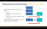
At least once if not more, many of us may have faced the following situation. We download the latest software driver for a device only to find out after installing that it doesn’t work for your hardware. As per the release notes, it should work for your hardware but in reality it does not. We have no choice but to revert back to the earlier… Read More
Future of Semiconductor Design: 2022 Predictions and Trends
Predictions and trends create the forces that accelerate innovations and keep the industry moving forward. We are all used to hearing of important issues and challenges, usually in the context of solutions offered by various vendors. The SemiWiki forum plays its role in bringing awareness of all of the above to its audience. For… Read More
Podcast EP18: The Story Behind Combining Methodics and Perforce
Dan and Mike are joined by Simon Butler, founder of Methodics and Brad Hart, CTO of Perforce. We explore the acquisition of Methodics by Perforce, including motivation, strategy and a look to the future. We also discuss some of the history of Methodics and how they became successful.
Single HW/SW Bill of Material (BoM) Benefits System Development
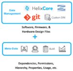
Most large electronics companies take a divide and conquer approach to projects, with clear division lines set between HW and SW engineers, so quite often the separate teams have distinct methodologies and ways to design, document, communicate and save a BoM. This division can lead to errors in the system development process,… Read More
Conference: Embedded DevOps

The catchy phrase DevOps is defined by Agile advocates as, “The practice of operations and development engineers participating together in the entire service lifecycle, from design through the development process to production support.”
I’ve been developing software since the stone ages, which means… Read More
Perforce Software Acquires Methodics!

This has got to be one of the most interesting and disruptive EDA acquisitions I have seen in some time. Another one that comes to mind is Siemens acquiring Mentor Graphics. We have been covering EDA PLM companies since the start of SemiWiki and have worked with most of them. If I had to keep score I would say it’s about even but … Read More
SEMI Takes the Jim Hogan and Simon Butler Conversation Virtual

As I originally reported a few weeks ago, the Jim Hogan fireside chat with Methodic’s CEO and founder Simon Butler was moved to a virtual event on May 1. The event was produced by the Electronic System Design (ESD) Alliance, a SEMI Strategic Technology Community. Bob Smith, executive director of ESDA, moderated the event. I am happy… Read More