High-speed digital (HSD) designers have long tested the limits of realizable speed. GHz frequencies are now the norm, and multi-level signaling is pushing rates higher while the long-awaited transition to optical signaling and even higher rates looms ever closer. Power density is also climbing, and data-hungry applications like AI unexpectedly create bottlenecks in power delivery with decreasing margins on sub-1V power rails carrying thousands of amps into large chips. The demands of signal integrity, power integrity, and electromagnetic interference (EMI) engineering are fueling a new generation of streamlined EDA workflows looking to deliver a high-fidelity, end-to-end digital twin from one simulation environment.
Keysight’s Advanced Design System (ADS) platform has set the industry standard for high-speed digital and power integrity design workflows with in-situ chip and printed circuit board (PCB) EM extraction and simulation. ADS has always prioritized simulation accuracy, combining classic circuit analysis with high-fidelity EM models in a co-simulation approach. It quickly delivers digital twin levels of accuracy, with more detailed results and design insights than extensive physical measurements, which can be challenging to set up, costly, and time-consuming. ADS R&D teams are now breaking new ground with more capabilities to find, visualize, and solve the root causes of complex design failures – before designers commit to hardware.
Keysight EDA teams previewed DesignCon 2025 and Keysight Education Forum technical talks on four design challenges ADS uniquely targets: advanced crosstalk analysis in wide-bus scenarios, 2kAmp power delivery for massive 3DHI chips, analyzing PCIe links with PAM4 modulation, and system simulation and verification of LPDDR5 designs used in AI applications.
One-pass crosstalk analysis for single-ended buses saves costly respins
A simplified view of crosstalk looks at only adjacent lines and judges the goodness of eye patterns. However, Hee-Soo Lee, HSD Segment Lead at Keysight, says customers indicate that tapeouts of dense, high-speed designs fail more often because of complex crosstalk problems – and identifying the culprits can be challenging. “Designing and laying out a complex board with a very wide single-ended bus can be tough, and designers must be mindful of avoiding unwanted design failures due to crosstalk-related eye closure,” says Lee. “Packages and vias on multi-layer boards can inject crosstalk to any victim line, not only from adjacent transmission lines, and with reduced design margin and higher data rates, even 10mV of crosstalk voltage may affect a system’s performance significantly.” If eye patterns look good, there’s no problem, but where and how does a designer go about fixing things if the eye is closed?
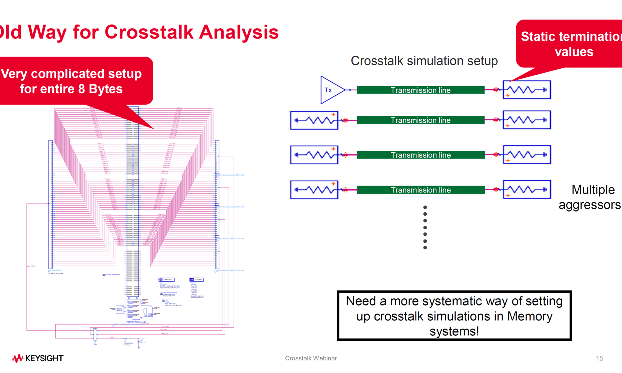
“With a 64-bit wide bus, it can be days just manually setting up crosstalk simulation runs,” continues Lee. “Correctly terminating multiple lines is tedious, and one can’t assume terminations are always 50 ohms – it depends on the drivers and receivers and the signaling conditions. One setup gets an answer for one aggressor and multiple victim lines, and then that process needs to be repeated perhaps 150 or 160 times to analyze the entire data bus.” Lee points out that in chip designs, things get even more complicated and can trigger a million-dollar re-spin of die or packaging if the analysis is not done right.
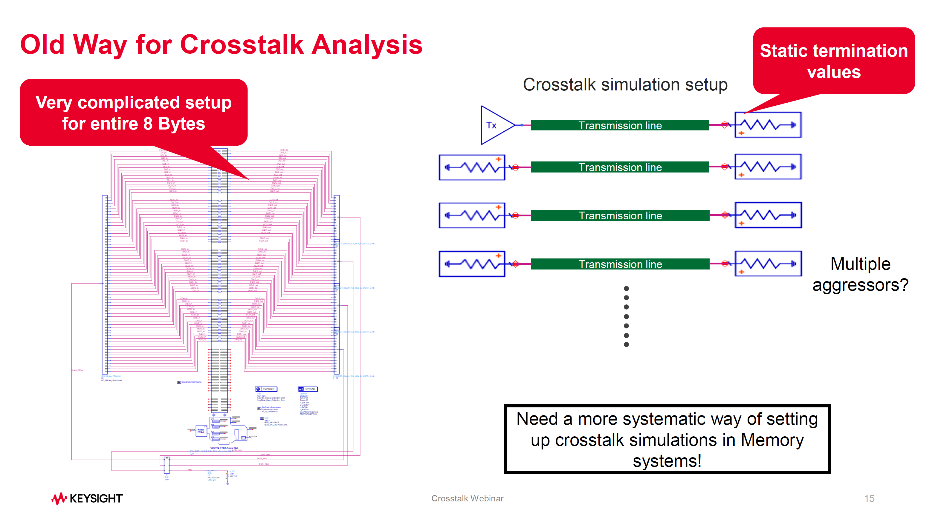
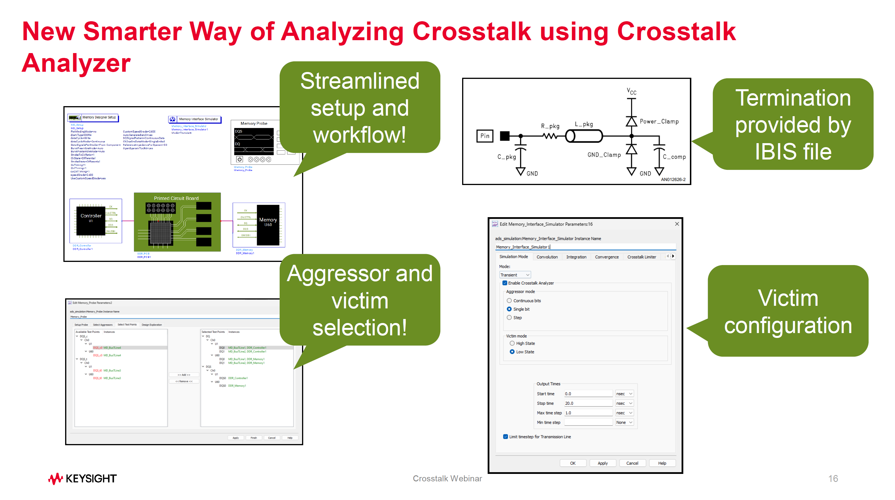
Keysight’s answer is Crosstalk Analyzer, now in the ADS 2025 release, with three unmatched values. First, it uses the IBIS termination model for the drivers and receivers to model terminations accurately, removing the guesswork. Second is the automated workflow for setting up a bus for crosstalk analysis with all aggressors and victims configured. Third are the versatile aggressor modes available, which include rising and falling steps, single pulses, and continuous signals. After this streamlined setup, ADS Crosstalk Analyzer simulates near-end and far-end crosstalk over the entire bus with the correct termination impedances for the signaling context in one pass directly from a single schematic.
“Tools are tools, and we still need engineers to find and fix issues,” adds Lee. He cites a test case from a customer’s example, a board with a memory interface running at 3200Mbps where crosstalk on a line came predominately not from the adjacent trace but from a via farther away, influenced by the BGA package and other vias in the board layout. “We produce meaningful data from automated crosstalk analysis in a few minutes, whereas other error-prone setups can take days and may not highlight the root cause of eye closure.”
Power integrity analysis in 1000A/nsec PCB power delivery network
Speaking of complex packages and multi-layer board layouts with vias, power integrity is also seeing issues stemming from board structure complexity. “Power delivery isn’t DC. It’s AC,” says Heidi Barnes, Sr. Application Engineer at Keysight. “For years, power delivery network (PDN) impedance typically registered as 10s of milliohms. Now, a server-class AI chip consuming 1600W requires PDN impedance in microohms, and suddenly, intentional structures and parasitics in multi-layer PCB and package layouts make a big difference.”
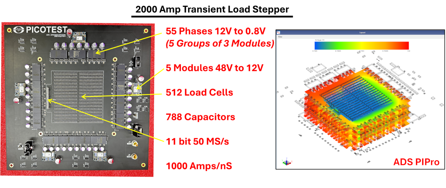
Barnes teams with Steve Sandler of Picotest and Ben Dannan of Signal Edge Solutions to highlight an interesting specimen – a 2000A, 11-bit programmable transient load stepper. Its claim to fame is slewing 1000A of load in one nanosecond. That figure seems otherworldly until one steps back to think about power management and sequencing, rapid switching of many transistors simultaneously, and inrush currents held up by bypass capacitors. It’s more realistic considering today’s large 3DHI chips and the concept of point-of-load power delivery, where rails must enter on some pins toward the center of a package for power integrity, transferred up from lower layers using vias. Barnes helped create a digital twin of the stepper in ADS PIPro for complete EM and electrothermal analysis.
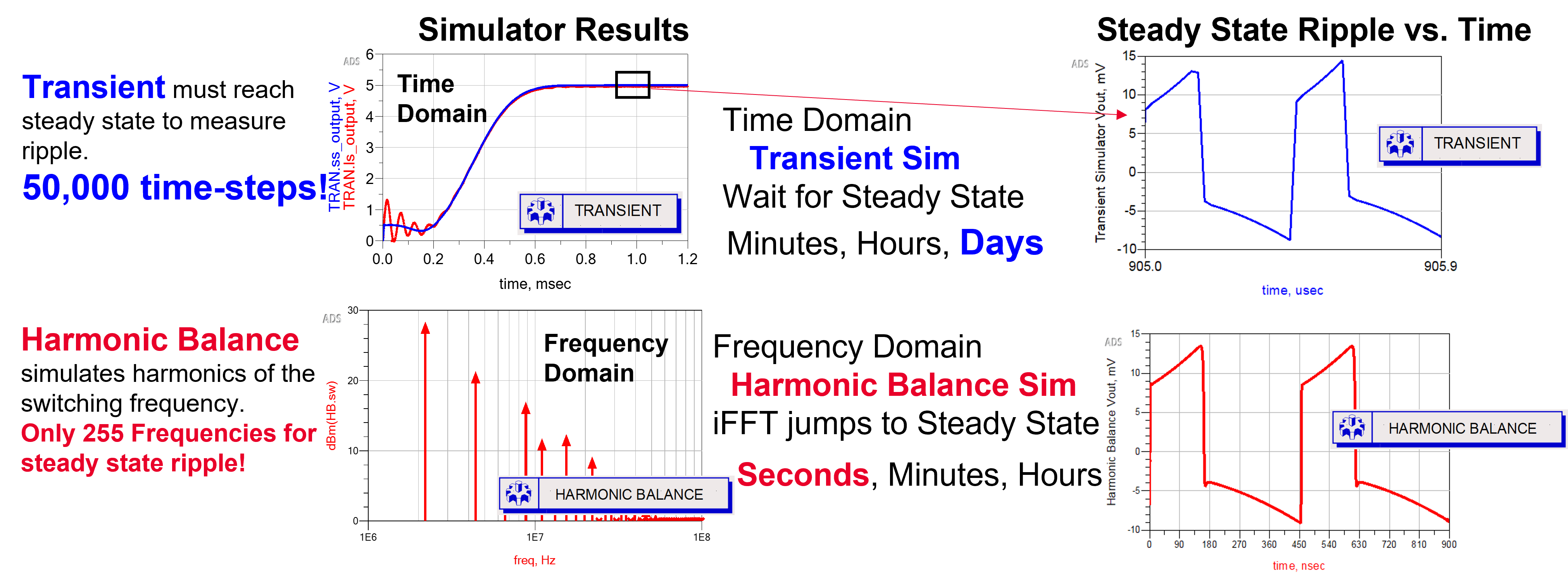
“People may not realize that 10 microohms of impedance on a power rail is sensitive to parasitic inductances of only 100 pH. Now we’re looking at transmission line effects in the kHz range,” continues Barnes. “Validating a power rail for stability used to imply small-signal AC analysis. But to understand these large dynamic loads, with crosstalk and ripple, and where to place things like sense lines, we’re turning to large-signal AC analysis.” Behavioral models of voltage regulator modules (VRMs) traditionally run in SPICE simulators can migrate to ADS frequency domain harmonic balance analysis for large-signal simulations that jump directly to the time domain steady-state ripple solution.
ADS PIPro simulations for this 2kAmp digital twin with 55 VRM phases run in 77 seconds, uncovering and visualizing a resonance from an impedance peak at 91 kHz. “When expensive devices are on the line, like in defense and aerospace applications, engineers need to look at this kind of power integrity simulation to reduce re-spins and prevent inadvertently exceeding a chip’s voltage or thermal reliability specifications,” concludes Barnes.
Pushing PCIe links faster and helping AI chipsets and systems scale
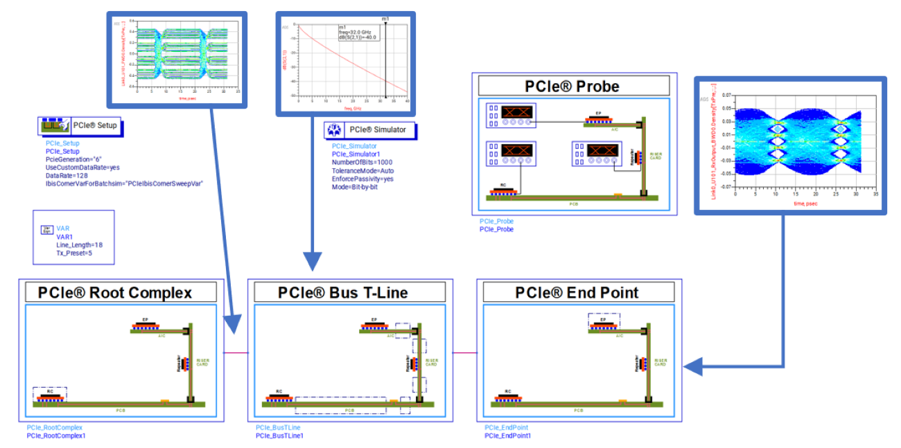
Two more high-speed digital topics look at the evolution of PCIe and the challenge of distributed LPDDR5 interfaces typical in AI applications. Pegah Alavi, Sr. Application Engineer at Keysight, is in a panel session with Samtec, Amphenol, and others, showing recent work with ADS looking deeper at PAM4 modulation used in PCIe 6.0 and other specifications and the impact of channel length and connectors as data rates increase to 128GT/s in future releases. Alavi emphasizes Keysight’s unified measurement science approach, sharing that PCIe compliance test solutions in Keysight real-time oscilloscopes also appear in ADS for use with simulated waveforms. Initial work on PAM4 simulations with 128GT/s data rates is complete, with equalization and channel characteristic enhancements in discussion for future generations of PCIe.
In a separate Keysight Education Forum technical talk, Alavi shares her collaboration with a partner company to develop promising ADS analysis results on power-aware LPDDR5 implementations, finding accurate target Z impedance values for optimizing eye diagrams. “We have a customer designing large AI chipsets, and the punchline is by using ADS, they spotted problems in simulation before fabricating their board prototypes,” she says. Much of the work analyzes trace spacing for crosstalk improvements, but another exciting result is a significant reduction in bypass requirements. “With data in hand, our customer cut bypass capacitors on the board by a bit over two-thirds, from 79 to 25. The analysis reduces BOM costs for the board and improves confidence in design margins for the LPDDR5 buses.”
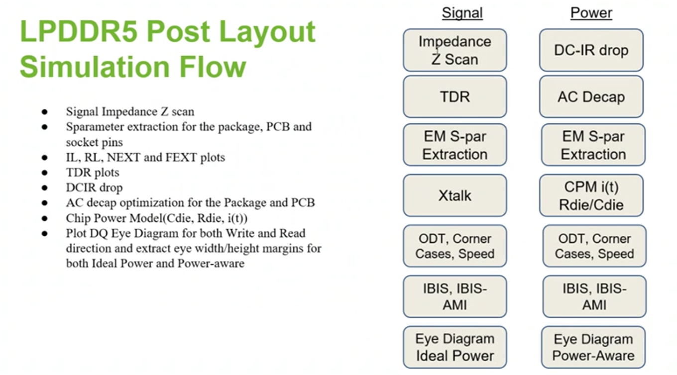
“Within a single design platform – ADS – combining memory design, signal integrity, and power integrity analysis, we can explore the LPDDR5 design space much more. That will help AI and other 3DHI chipset designs scale faster while delivering first-pass silicon and board success,” Alavi concludes.
Learn more at DesignCon 2025 and KEF
More details will come in tutorial and panel sessions at DesignCon 2025 and the Keysight Education Forum sessions at the Santa Clara Convention Center. In addition to the speaking slots on the program, exhibitor attendees can see Keysight’s ADS with power and signal integrity solutions and its Chiplet PHY Designer in booth #1039. For more information, please visit the following:
Keysight ADS 2025 Product Release
Keysight Expands Chiplet Interconnect Standards Support in Chiplet PHY Designer 2025
Also Read:
Chiplet integration solutions from Keysight at Chiplet Summit
GaN HEMT modeling with ANN parameters targets extensibility
Keysight EDA 2025 launches AI-enhanced design workflows
Share this post via:


Comments
There are no comments yet.
You must register or log in to view/post comments.