Layout parasitic extraction (LPE) has three primary goals – accuracy, capacity, and throughput. Traditionally, LPE tools have offered two methods for capacitance derivation, with tradeoffs on these goals:
- a 3D field-solver algorithm
The detailed 3D topology of interconnects and dielectrics are presented to an algorithm which solves electrostatic equations for capacitance calculation – either a differential or integral form of Maxwell’s equations could be used.
- application of empirical formulas, from representative layout topologies
Due to the complexity of VLSI interconnects, this method is commonly used. A set of layout patterns are analyzed using a field-solver algorithm, and fitting parameters are derived to provide capacitive formulas. From this pre-characterized set of topologies, LPE tools perform a general pattern match, submitting the specific interconnect dimensions to the formulas, to calculate capacitance values by interpolation. Accuracy is reduced, yet the capacity and throughput are significantly improved.
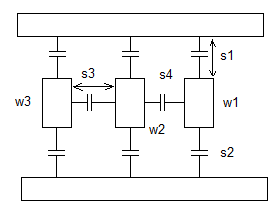
Figure 1. Empirical formulas are developed with width, space, and length fitting parameters for extraction using layout pattern template matching techniques
Yet, what about the circuit structures where extraction accuracy is paramount? Field-solver (FS) algorithms are required. There are various types of 3D field solvers for layout parasitic extraction, with performance/accuracy tradeoffs depicted below:
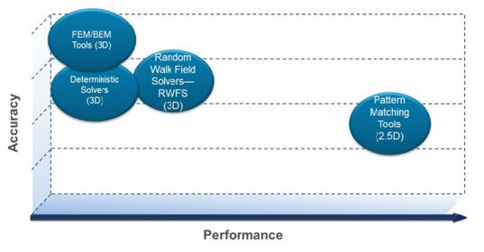
Figure 2. Illustration of layout parasitic extraction algorithm performance/accuracy tradeoffs.
Boundary Element Model (BEM)
Many initial implementations of FS-based capacitance extraction used a Boundary Element Model (BEM) algorithm, which utilizes the integral equation method. This enables the use of a surface model for the charges, electric fields, and voltages in the interconnect topology.
Recall from electrostatic theory that a (fixed) charge emanates an electric field (vector); the potential difference (scalar) between two points in the integral of that field, as illustrated in the figure below.
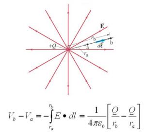
Figure 3. The potential difference between two points depends upon the integral of the electric field, emanating from electrostatic charges; this example depicts a fixed point charge in free space
Specifically, note the (1/distance) dependency for the potential difference from the location of the fixed charge.
Expanding this definition to an integrated circuit, the potential difference between two wires is related to the integral of the electric field emanating from one to the other, over the entire surface area of the wires. In a multi-conductor model, the calculation of these electric fields (from the local charge density on each wire) represents a complex system that requires a concurrent solution for all wires.
The goal of BEM capacitance extraction of a general 3D structure is to translate the familiar relation: C = Q/V , into an equivalent model.
The BEM method commonly uses an indirect approach — i.e., assume a potential difference between all wires, then solve the entire system for the (total) charge on each wire. The voltage difference is still on the “left-hand side” of the equation, as illustrated above, with a set of equations to be solved for the charge on each wire.
For example, given a set of interconnects, assume a voltage difference of V = 1 Volt between a reference conductor “i” and all other wires (at 0 V), and solve the system for Q_total on each other wire, which also solves for Cij between wires. Superposition theory is applied, enabling the calculation to iterate through each interconnect as reference to complete the Cij capacitance network.
In general, the extraction model will involve many interconnects, with strong interactions between all surfaces. As a result, the integral equation to solve for the electrostatic charges for all the conductor surfaces is intractable.
The BEM method discretizes the surfaces of all the conductors in the model into a set of tiles, and assumes the charge is uniformly distributed across the area of each tile. The figure below illustrates the BEM concept, for the simple case of two interconnects.
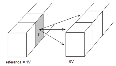
Figure 4. The complete BEM interconnect model divides all conductors into tiles, with uniform charge density assumed across the tile; a reference interconnect is set to 1V, with all other interconnects at 0V.
The BEM method calculates the summation of the charge Q on all tiles for each interconnect “j” at 0V, from the set of tiles on the reference interconnect “i” at 1V, to determine their capacitance, Cij. The LPE tool then iterates through all interconnects as reference, to develop the full capacitive network (and then incorporates the resistive segment values, to provide an RC network as the parasitic netlist output).
For each reference, this discretization approach generates a dense matrix of coefficients to solve the equation for the charges on the individual tiles:
P*q = v
where v is a Nx1 vector of (known) voltages on each of the “N” tiles in the model, q is the Nx1 vector of charges on each tile to solve, and P is a matrix of size NxN that represents the (1/distance) dependency of the contribution of the charges on each tile to the potential on another tile.
Solving this BEM matrix equation for each reference is computationally demanding, both in computer time and memory. This has severely limited the applicability of FS algorithms to all but the simplest layout cells and patterns.
Floating Random Walk (FRW) Field Solver Method
An alternative approach to calculating interconnect capacitance has emerged.
The floating random walk (FRW) method uses a “walking set” of (conductor-free) 3D cubes between interconnect surfaces to (recursively) solve for the charge density and thus capacitances. [ References 1, 2 ]
This method does not require building a full discretized interconnect matrix model to solve, but rather uses a set of statistically-sampled paths between conductors to derive an estimate of the overall potential distribution. From the potential data, the electric field (gradient of the potential) and interconnect charge density (surface integral of the electric flux) are calculated.
To achieve high accuracy of the electrostatic potential calculations, a large number of path samples originating from the reference conductor and terminating on other interconnects is required.
The compute time is equal to: T = (# of paths) * (average # of hops/path) * (time per hop), where the time per hop is dominated by the geometric calculation of the size and direction for the next cubic surfaces in the path.
Of specific note is that the FRW method does not require massive memory storage for matrix calculations related to the complete discretized interconnect model, unlike the BEM method described above. And, it is extremely parallelizable.
Cadence Quantus FS
I had the opportunity to chat with Hitendra Divecha, Product Management Director, and Hao Ji, Software Engineering Group Director, for the Digital and Signoff Group at Cadence. They were excited to share details of a new FRW field-solver extraction product release, Quantus FS.
“With the parallelization features incorporated into Quantus FS combined with a cloud computational model, we are now able to provide a field-solver approach for large layout extraction.”, Hitendra indicated. “The days of compromising accuracy vs performance for a 3D field solver are behind us now.”
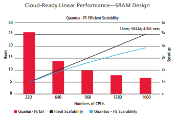
Figure 5. Quantus FS runtime scalability (up to 1600 CPU’s!), for a 16nm SRAM macro with 4.5M nets.
The capability to submit large macro layouts to FS-level accurate extraction will be a game-changer for (SRAM and mixed-signal) IP parasitic extraction. Designers who are using conventional extraction methods, or pursuing a complex methodology with FS algorithms used on small layout cells stitched into larger non-FS models, will now have the opportunity to realize all three extraction goals — accuracy, capacity, and throughput.
Quantus FS can be leveraged for standard cells, SRAM, other memory such as DRAM, MRAM, flash, etc., AMS and Interface IPs, automotive sensors, touch display and LCD/TFT designs and any sensitive circuits that must extract highly accurate parasitics.
For more information on Quantus FS, please follow this link.
-chipguy
Reference 1: Y. Le Coz and R. B. Iverson, “A stochastic algorithm for high-speed capacitance extraction in integrated circuits“, Solid State Electronics, Vol., 35, No. 7, pp. 1005-1012, July, 1992.
Reference 2: Wenjian Yu, et al., “RWCap: A Floating Random Walk Solved for 3-D Capacitance Extraction of Very-Large-Scale Integration Interconnects”, IEEE Trans. on Computer-Aided Design of Integrated Circuits and Systems, Vol. 32., No 3, pp. 353-366, March, 2013,
Share this post via:


Comments
3 Replies to “Field-Solver Parasitic Extraction Goes Mainstream”
You must register or log in to view/post comments.