Earlier this year. as part of my coverage of the virtual Design Automation Conference (DAC), I interviewed Agnisys CEO and founder Anupam Bakshi. He talked about the new products they introduced at the show and filled me in on the history of the company and his own background. Recently, Anupam presented the webinar “System Development Using Agnisys” and I was curious about their status so I checked it out.
My main impression is that the company has done a nice job of moving beyond focusing on individual products to show how they can be used together in chip development. I think that’s important for two reasons. First, Agnisys has quite a few products for a relatively small company. I count eight products or product families, with some variations. For example, their flagship IDesignSpec™ (IDS) is available as a Microsoft Word plug-in, a Microsoft Excel plug-in, a batch tool, or their new IDS NextGen GUI and executable specification editor. For users looking to solve a specific design or verification problem, it seems clear from their website what product to choose.
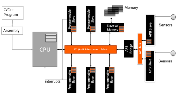
It’s also important to show users how Agnisys tools fit together in a flow to contribute to the overall design and verification effort, and I was pleased to see that the recent webinar addressed exactly that topic. The focus was on the design and verification of embedded systems, which is a broad topic. Anupam noted that the system-on-chip (SoC) hardware design can use ASIC or FPGA technology and include a wide range of IP from internal teams, commercial providers, and open-source projects. The software components include firmware and device drivers that interact closely with the hardware and extend up to the operating system and applications. I was impressed that the company covers so much of the embedded hardware-software spectrum.

The webinar then discussed some of the design and verification challenges for SoC development, identifying specification changes as a major problem. That seems accurate to me. Every time that the architecture spec is updated, it has ripple effects to the hardware design and, quite often, requires software updates as well. Both the hardware and software must be re-verified to test the changed functionality and ensure that nothing was broken by the updates. Then the entire system must be validated, consuming expensive resources and delaying tapeout. These issues are bad enough, but it’s even worse when the teams get out of sync. This is hard to avoid when the spec changes are communicated to the engineering groups at different times and implemented on different schedules.
It seems to me that automating the design and verification process from executable specifications is the key to the Agnisys solution. Their tools generate RTL design code, verification testbenches and tests, device drivers, documentation, and even programs that can be used to test the fabricated chips. Obviously, this saves a lot of time and money, but it also ensures that all development teams remain in sync. Specification changes are propagated immediately to all stakeholders with the simple push of a button in the GUI or a simple command in batch mode. Agnisys automates the design and verification of registers, memories, sequences, bus interfaces, and several types of IP. They also provide tools to connect all these elements, plus user-developed blocks, into a complete SoC.
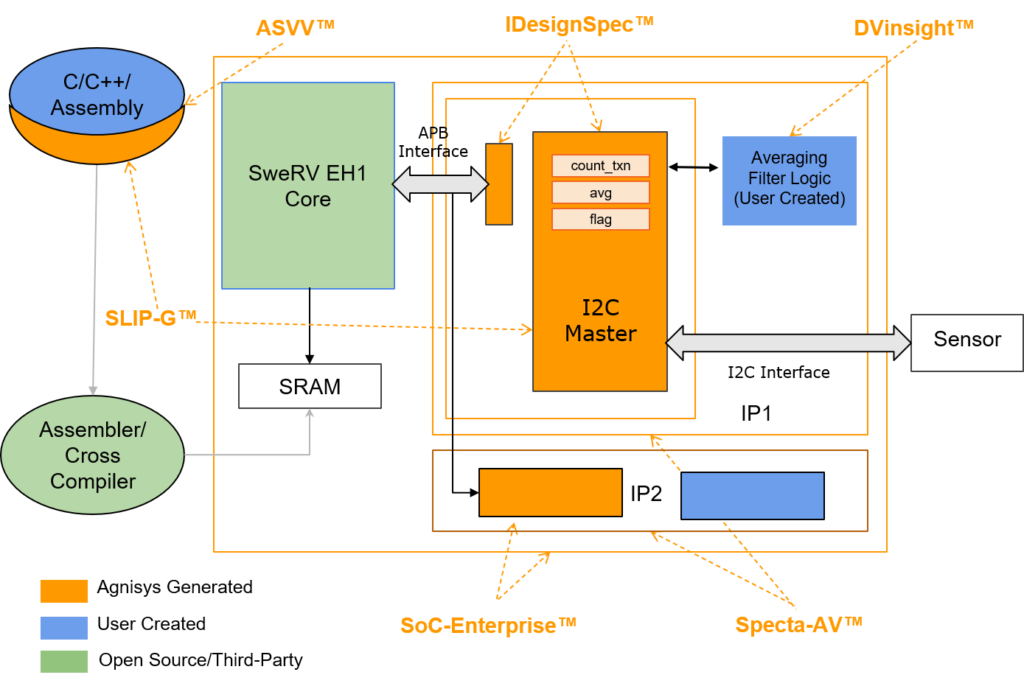
What I liked best about the webinar is that it wasn’t a pitch for Agnisys products, full of features and benefits. Instead, the team put together a small but realistic SoC design and walked us through the process of using Agnisys tools within an embedded systems development flow. The design averages sensor data received over an I2C interface. Sensor values are read in and converted into an averaged value by user application logic, all under control of software running on a CPU. Anupam showed the input specification formats and the different types of code automatically generated at each stage of the process. I appreciated seeing these technical details rather than just a bunch of sales slides, although I wish that they also showed some of the tools running.

I’d like to thank Agnisys for alerting me to this webinar and for putting together quite an interesting event. If you missed it you can register to watch the recorded version here. I hope that you find it as interesting as I did.
Also read:
Automatic Generation of SoC Verification Testbench and Tests
Register Automation for a DDR PHY Design
CEO Interview: Anupam Bakshi of Agnisys
Share this post via:


Musk’s Orbital Compute Vision: TERAFAB and the End of the Terrestrial Data Center