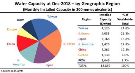
Semiconductors are not only critical to modern life, semiconductors are critical to National Security. Now that leading edge semiconductor foundries have left the United States one of the more pressing challenges is secure semiconductor manufacturing. This applies to all countries of course so let’s take a look at the International wafer capacity landscape:

One thing that we should note here is Government semiconductor industry support. Taiwan, Korea, China, and even Japan have significant government support for semiconductor manufacturing. Europe and the United States not so much. In fact, here in the United States semiconductor manufacturing is going the way of the dinosaur. My guess is that Asia and China specifically will continue to chip away at global wafer capacity leaving the US figuratively fabless, absolutely.
All is not lost of course because in my experience semiconductor professionals are the smartest people in the world and will not be defeated by political ignorance. One example is physical design for secure split manufacturing ICs. This is not new but now the NSF is getting involved so it is getting real:
Award Abstract #1822840
STARSS: Small: Collaborative: Physical Design for Secure Split Manufacturing of ICs
Abstract—The trend of outsourcing semiconductor manufacturing to oversea foundries has introduced several security vulnerabilities — reverse engineering, malicious circuit insertion, counterfeiting, and intellectual property piracy — making the semiconductor industry lose billions of dollars. Split manufacturing of integrated circuits reduces vulnerabilities introduced by an untrusted foundry by manufacturing only some of the layers at an untrusted high-end foundry and the remaining layers at a trusted low-end foundry. An attacker in the untrusted foundry has access only to an incomplete design, and therefore cannot easily pirate or insert Trojans into it. However, split manufacturing alone is not sufficiently secure, and naïve security enhancement techniques incur tremendous power, area, and delay overhead. The goal of this research is to develop new physical-design techniques that can ensure security through split manufacturing and simultaneously minimize the overhead on performance, power and area of semiconductor products.
This research lays the foundations for a comprehensive set of physical design tools for security. Its expected outcomes are: 1) Systematic techniques for modeling attacks that recover the missing parts of the design from the information available to the attacker; 2) Security metrics to assess the strength of integrated circuit designs by measuring the difficulty for an attacker to reverse engineer the design in the context of split manufacturing; 3) Active defenses through physical designs techniques such as cell layout, placement perturbation and rerouting designs to increase security; 4) Techniques to reduce the overhead of secure split manufacturing and make the security enhancement seamlessly compatible with existing design flows.
And here are a couple of background papers:
Building trusted ICs using split fabrication
Abstract— Due to escalating manufacturing costs the latest and most advanced semiconductor technologies are often available at off-shore foundries. Utilizing these facilities significantly limits the trustworthiness of the corresponding integrated circuits for mission critical applications. We address this challenge of cost-effective and trustworthy CMOS manufacturing for advanced technologies using split fabrication. Split fabrication, the process of splitting an IC into an untrusted and trusted component, enables the designer to exploit the most advanced semiconductor manufacturing capabilities available offshore without disclosing critical IP or system design intent. We show that split fabrication after the Metal1 layer is secure and has negligible performance and area overhead compared to complete IC manufacturing in the off-shore foundry. Measurements from split fabricated 130nm testchips demonstrate the feasibility and efficacy of the proposed approach.
Published in:2014 IEEE International Symposium on Hardware-Oriented Security and Trust (HOST)
Is Split Manufacturing Secure?
Abstract—Split manufacturing of integrated circuits (IC) is being investigated as a way to simultaneously alleviate the cost of owning a trusted foundry and eliminate the security risks associated with outsourcing IC fabrication. In split manufacturing, a design house (with a low-end, in-house, trusted foundry) fabricates the Front End Of Line (FEOL) layers (transistors and lower metal layers) in advanced technology nodes at an untrusted high-end foundry. The Back End Of Line (BEOL) layers (higher metal layers) are then fabricated at the design house’s trusted low-end foundry. Split manufacturing is considered secure (prevents reverse engineering and IC piracy) as it hides the BEOL connections from an attacker in the FEOL foundry. We show that an attacker in the FEOL foundry can exploit the heuristics used in typical floorplanning, placement, and routing tools to bypass the security afforded by straightforward split manufacturing. We developed an attack where an attacker in the FEOL foundry can connect 96% of the missing BEOL connections correctly. To overcome this security vulnerability in split manufacturing, we developed a fault analysis-based defense. This defense improves the security of split manufacturing by deceiving the FEOL attacker into making wrong connections.
Published in:2013 Design, Automation & Test in Europe Conference & Exhibition (DATE)
Bottom line:
The need for a trusted foundry source at advanced process nodes will require unique fabrication methods, utilizing split manufacturing. There are numerous technical challenges:
- defining the appropriate FEOL and BEOL layers for the split
- coordinating the lithography alignment and depth-of-field requirements between foundries at the split
- ensuring compatibility of the passivation and interconnect material(s) between foundry processes
- defining incoming wafer inspection procedures at the BEOL, both metrology and electrical characteristics
These fabrication challenges are daunting, but solvable. A greater issue is how to ensure the FEOL data provided to the untrusted foundry cannot be easily reverse-engineered, and that the subsequent FEOL processing does not incorporate any unwanted, latent logical or electrical behavior. The detection of a potential “Trojan” inserted into a design to cause erroneous system behavior in the field is paramount.
As mission-critical electronics advances to new process nodes, it will be very interesting to see how both the design and fabrication aspects of split manufacturing evolve.
Share this post via:


Musk’s Orbital Compute Vision: TERAFAB and the End of the Terrestrial Data Center