 A few weeks back I wrote an article mentioning that Mentor Graphics has been quietly working on solutions for photonic integrated circuits (PICs) for some time now, while one of their competitors has recently established a photonics beachhead. One of the most common challenges for PIC designs is their curvilinear nature, thus the reference to the now infamous battle of the bulge. To continue the parlance, Mentor has, in fact, been attacking PIC design on multiple battle fronts. Don Dingee wrote a nice article about one of those efforts in which Mentor’s Tanner team has been working with Luceda to make photonic design more straightforward (see link below).
I also wrote an article highlighting some of Mentor’s efforts in the area of Electro-Optical Design using their Pyxis and Calibre tool sets. The one point that hasn’t really been made in these articles, though, is that Mentor’s Calibre design rule checking (DRC) and layout-vs-schematic (LVS) technologies hold a strategic articulation point for any design going into a silicon-based foundry. Calibre is the de facto sign-off DRC & LVS tool for all production silicon foundries, and as silicon photonics starts to take hold, it will be essential that those foundries have good photonic DRC & LVS rule decks in place. Turns out this is a bit trickier than one might imagine. The good news is that Mentor has been working on this now for more than five years, and they have built up a wealth of experience.
As mentioned, the challenge when doing DRC for PICs is the curvilinear data, the aforementioned bulge. These curves get digitized into polygons with thousands of points that represent the curves in a piece-wise linear fashion, each of which must be snapped onto a manufacturing grid. The result is that a normal DRC deck will report thousands of false errors from these highly discretized shapes.
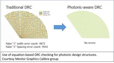
The example picture on the left from one of Mentor’s silicon photonics white papers shows concentric circles very typical of a photonics design style used to make spiral delay lines. Note the thousands of colorations along the design shapes denoting error markers from DRC using a normal DRC deck. The picture on the right is the same set of concentric circles, but now they are DRC clean. In this case, the Calibre team used their experience to modify the DRC deck to redefine the rules for width and spacing, given the knowledge that these shapes were indeed digitized curves with a given radius of curvature and spacing.
Two things were needed to make this happen. The first is that information needed to be sent to Calibre tools so that they knew to treat these shapes differently. This was done by a flow that Mentor put together with PhoeniX Software, which is used in Mentor’s Pyxis flow to generate these types of shapes. The second thing that needed to happen was to have a DRC capability that could use the information forwarded from PhoeniX to perform a type of check that was amenable to the identified shapes. Mentor put their equation-based DRC capabilities to work to solve this problem.
A second challenge for PICs is how to best perform LVS. The good news is that PIC designers are now using a PDK approach to building their designs. This means that many of the tricky LVS challenge can be subsumed within the PDK components. This includes things like logical connections between waveguides that transfer data through evanescent coupling where the waveguides don’t actually touch. These connections become components with pins, as opposed to the LVS tool having to discern a coupler vs. two waveguides simply passing each other. This makes the checking of basic connections easier, especially if one has a schematic with which to compare.
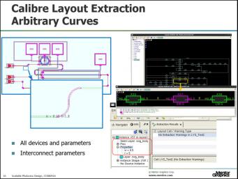 Another photonic LVS problem is checking schematic parameters against the layout. In electronic ICs, this would be comparable to measuring transistor widths and lengths in the layout and then comparing them to the W and L parameters in the schematics. With PICs this is much harder, as the parameters are not simple scalar values, but instead mathematical relationships. This has been a research subject of groups like PLAT4M (of which Mentor has been a member), and Mentor has come up with some unique and powerful solutions to these problems.
One solution, as already mentioned, uses forward-annotated data where Calibre compares the layout to a rendering based on the forward-annotated equations. This can be done using a combination of Calibre’s Design for Manufacturing capabilities, including its YieldServer API and DFM database, and geometric operations in the Calibre DESIGNrev finishing tool. Additionally, Mentor has come up with a nifty way to do the equivalent of a geometric checksum on PDK components based on parameters as specified in the schematic. This checksum can be computed for the actual layout shapes found and compared against the logical checksums from the schematics, flagging layouts that don’t match their schematic counterparts.
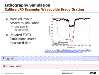 Rounding out Mentor’s photonic capabilities is the ability to use their Calibre LFD package to simulate a foundry’s lithography and etch processes to view how the actual manufactured layout will look. In this case, the designer can not only do DRC and LVS on these simulated shapes, but they can also generate data that can be back-annotated for re-simulation of both the components and the circuit as a whole. Through its collaboration with Lumerical Solutions, Mentor can back-annotate all measured shapes (lengths, widths, radius of curvatures, etc.) of the simulated manufactured design and send them to both Lumerical’s compact model generation process (to create updated S-matrix component models) and to Lumerical’s INTERCONNECT circuit simulator (for full circuit level simulations).
In cases where the design is known to be going into high volume production runs, these types of simulations can be done across the expected manufacturing process window to identify design areas that may be susceptible to yield fallout.
So, while the competition may have recently secured a photonic beachhead, Mentor Graphics has already pushed well inland and is driving forward on multiple photonic battlefronts, including the strategic articulation point between design and manufacturing.
See also: Electrical-Optical Design-A Bridge to Terabitsia and Making photonic design more straightforward
Share this post via:


Comments
There are no comments yet.
You must register or log in to view/post comments.