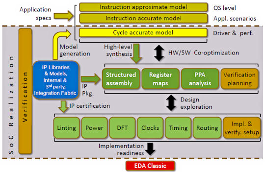


There are some very interesting comments to the last entry on SoC Realization and how more and more chips are actually assembled out of IP. There was clearly a lot of discussion in this area at DAC, although most people (Atrenta being an exception) don’t use the term SoC Realization, presumably because it was originated by Cadence. But just because there is a dysfunctional gap between what Cadence talks about in EDA360 and what they currently deliver doesn’t mean that the basic ideas are wrong. I’ve argued before that so far both Synopsys and Mentor are currently doing a better job at implementing the EDA360 vision than Cadence are themselves.
One of the point that several commenters made was that IP reuse is expensive, in the sense that if you design a block to be reused rather than just used in the chip you are working on then it will take more effort. Reuse seems to work best at the very low level (standard cells, memory blocks etc) and the higher functional level, the higher the better. Microprocessors obviously, but also large blocks like GPS or cable-modems.
One of the biggest challenges about re-use is that it really is expensive. Long before any of us had even thought about IP in semiconductors, Fred Brooks in his book The Mythical Man-month reckoned that a reusable piece of operating system code that had to run on a range of machines and be reliable, was 9 times more expensive than the quick-and-dirty bit of code that a programmer could come up with to solve their specific issue, a factor of 3 for flexibility and a factor of 3 for making it industrial strength. At a seminar in Cambridge (the real one!) where he was on sabbatical back then, I guess this must have been 1975, he said that he thought that the two factors of 3 should have been two factors of 5 and so it was actually 25 times more expensive.
When I was at VLSI Technology, we had blocks of reusable silicon that we called FSBs, for Functional System Blocks. We jokingly called the Fictional System Blocks since, in most cases, the work to make them reusable (models, vectors etc) didn’t yet exist. The block did genuinely exist, and had seen silicon, but it would be too expensive to make all the blocks resuable without a customer. Instead, we did a sort of just-in-time reusability, making the blocks reusable once someone showed up and wanted to use them. Making all the blocks truly available at all the process nodes would have made the whole idea unprofitable.
3rd party IP, of course, typically comes with all that is required to use the block. The idea is that the cost of making blocks reusable is amortized across a large number of customers/designs. One problem is that often that is not the case, the design is used in just a very small number of designs in different processes, with a result that many IP companies really have more of a service business model (porting IP) than stamping out lots of pre-standardized product.
Nonetheless, most of most chips these days is IP that was either from a previous chip, or from a 3rd party. Very little is RTL written just for that one chip. SoC Realization, by whatever name, is the way many chips are designed.
Share this post via:


Consolidation and Competition: Who is Winning the $4.5 Billion Interface IP Race?