When I got the opportunity to blog about verification, I thought, what new and interesting things should I talk about? Having started my EDA career in 1983, I often feel like one of the “oldies” in this business…remember when a hard drive required a static strap, held a whopping 33 MB, and was the size of a brick? Perhaps they should get someone who has just a few less EDA miles on them? However, thinking further on it, “we veterans” have experienced big changes in design and verification and the impact that tools and technology have had in creating new devices and exciting new markets that are changing the way we live. We have a lot to share.

That’s why I’m initiating a series of blogs to discuss valuable insights into the methodologies, tools, and flows we will need to move into the next generation of high technology. I’ll begin with several blogs about a trend I am seeing now—further reducing the power in designs in a world of increasing performance using a fairly complex interaction of HW and SW. After looking at the most important trends in low power, we’ll broaden our conversation to encompass other trends in verification.
We are seeing that how a typical ASIC or SoC low power design is done is starting to change dramatically. Current low power design and verification methodologies are breaking down, with some of the most successful leading semiconductor companies even losing business because they did not reduce power enough. The traditional implementation-focused low power methodologies are being strained because they ignore a whole phase of the verification process—those that exist at the RTL or above. And companies everywhere are feeling the pain.
We need new low power methodologies, we need new tools and flows, and we need low power techniques that make it easier to incorporate low power design and verification very early in the design cycle. Waiting until the entire SoC/ASIC is assembled and implemented is not the best way to optimize for power. We are now seeing SoCs going from 10 to 100 power domains, which introduces a whole new level of complexity in the design. How do you know that you have properly verified all of the states and interactions? Should you have a methodology that considers low power coverage now?
It’s neither feasible, nor prudent, to wait until the back end of the design flow to start paying attention to low power design techniques and their validation, as it is done presently. Too many interactions with lower power circuitry are missed, and it is too late to make design changes that either fix bugs introduced by low power cell insertions or optimize the balance between power, performance, and area. You need to move up in abstraction and have the tools that support there. You need to start thinking about power at the RTL or above.
First of all, we need to take full advantage of new capabilities in the Unified Power Formant (UPF) that allow you to begin power management at a higher level of abstraction. Up until now, the UPF has tended to be implementation-oriented. But describing power intent at this low-level of abstraction is inefficient, forcing power intent information to be managed across different stages of the design flow and across different implementations of a particular system.
EDA companies have been working diligently with the semiconductor industry to develop an enhanced and more useful standard that provides more capabilities. After all, you have to make sure that all of those things you’re doing to achieve lower power in your designs—like power gating, multi-voltage design, etc. —don’t screw everything up. Adding these to your design can essentially create a brand new design. So there are BIG differences between traditional simulation and low power simulation. You need to make sure you are using the best, and the appropriate, power aware tools and techniques in your entire verification flow—from simulation to formal to emulation.
As I implied, some of us may be old, but we “ain’t dead yet.” Our experience can help guide the industry toward a brave new technological world. In forthcoming blogs I’ll explore in more depth what’s changed in low power technology and what you need to look for in solutions you WILL need to stay nimble.
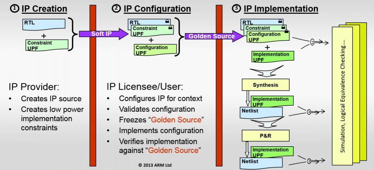
My next blog will look at what’s been happening in UPF to help facilitate the new wave of changes coming in low power solutions. We’ll delve into a new power-design methodology, called “successive refinement,” as used by ARM®, which integrates low power verification techniques starting from the IP block through SoC integration and implementation.
Subsequent blogs will talk about specific aspects of the successive refinement flow: things like issues with multi-clock domain designs when low power circuitry is introduced, what you should be looking for when debugging low power designs, the way you should approach low power coverage, and why you need emulation to for HW/SW co-simulation in a low power environment.
I would also like to hear your stories about your successes—and stumbling blocks—in our constantly and rapidly evolving electronic landscape.
Until next time, if you want to read a good overview of low power challenges and solutions, check out the on-demand web seminar “New Low Power Verification Techniques” at:http://www.mentor.com/products/fv/multimedia/new-low-power-verification-techniques
Share this post via:


Comments
There are no comments yet.
You must register or log in to view/post comments.