From Zion Research I learned that the flexible electronics market was about $13.2B in 2021 and growing at a CAGR of 21%, so that was impressive. There are several factors that make rigid-flex circuit so attractive, like: space efficiency, reduced weight, enhanced reliability, improved signal integrity, streamlined assembly, design flexibility, cost savings, miniaturization, and better durability. I learned more by reading a new eBook online.
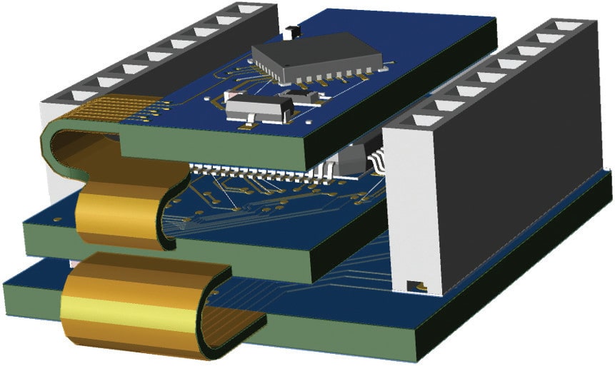
Wearable products like fitness trackers, smart watches and AR glasses have very limited space, so they benefit from space efficiency. Traditional PCBs use connectors and cables that add to product weight, so rigid-flex provides weight savings in markets like automotive and aerospace. Connectors and cables contribute to reliability issues, while rigid-flex designs are engineered to withstand bending and movement. With fewer electrical discontinuities, rigid-flex circuit exhibit improved signal integrity and impedance control, a benefit for high-speed and high-frequency products. Using less components to connect makes rigid-flex a simpler assembly process with lower costs from labor and materials. Engineers can design products with new shapes and configurations using rigid-flex, not possible with rigid PCBs, enabling new categories of products.
PCB design tools that support rigid-flex PCB need to manage layer stackups in both the rigid and flexible layers. Bend areas should be easily defined and visualized and must support the bend radius and fold lines. Components ought to be placed quickly in both the rigid and flexible areas, along with 3D visualization. Routing tools are required to support trace routing along the flex areas while maintaining signal integrity and allowing sketch or manual routing. Issues like excessive bending or trace spacing violations need to be found during Design Rule Checking (DRC). Both thermal and signal integrity simulations must be performed to ensure reliable operation. An accurate media library should include flexible materials and support both rigid and flexible substrates.

PCB designers use 3D visualization to best understand the entire rigid-flex PCB, along with bending simulations. An ideal EDA tool automatically generates fabrication and assembly drawings, detailing the flexible regions. Mechanical and electrical designers collaborate through import and export features. The best manufacturing yield is ensured when Design For Manufacturing (DFM) checks specific to rigid-flex are run. Using library components designed for flex circuits makes for quicker work.

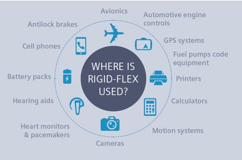
Rigid-flex technology is used in a wide range of markets as demands are growing for miniaturization, like for wearable smart products, automotive electronics, aerospace and defense, medical devices, consumer electronics, and IoT.

PADS Professional
Siemens offers their PADS Professional software as a solution to rigid-flex PCB design challenges that have been discussed so far. The approach with PADS Professional is to use a correct-by-construction technology, which enables your design team to create an optimal form factor with high quality, in the shortest time frame.

With this EDA tool PCB designers can define unique stack-up types, specify bend areas, and use flex-aware placement and routing to get high quality results. Both 3D bending and 3D DRC are supported, eliminating surprises in fabrication. Signal Integrity and Power Integrity are validated quickly through simulations. DFM validation understands rigid-flex and your designs are readied for NPI hand-off.
Summary
So much of our consumer electronics, automobiles and aircraft are already using rigid-flex technology and the market projections show a healthy growth for years to come. There are many challenges to adopting a rigid-flex PCB design flow, so you really want to adopt technology that is well proven over many years, designs and industries. With PADS Professional there is solid technology to address each of the challenges of rigid-flex PCB design.
Read the complete 7 page ebook online at Siemens.
Related Blogs
- Why Use PADS Professional Premium for Electronic Design
- EDA in the Cloud with Siemens EDA at #59DAC
- Interconnect Choices for 2.5D and 3D IC Designs
- Mainstream PCB Design Requires a Complete Tool Platform, Too
- Developing Affordable IoT Systems


Comments
There are no comments yet.
You must register or log in to view/post comments.