Last week I talked with two experts at Mentor about the challenges of getting IC designs into the 32nm/28nm node on the Common Platform (IBM, GLOBALFOUNDRIES and Samsung). Global Foundries issued a press release talking about how the four major EDA companies have worked together to qualify EDA tools for this node.

Sudhakar Jilla, marketing director, P&R
Michael Buehler-Garcia, marketing director, Calibre
Retrospect
Back in 1986 I was designing a graphics chip at Intel using a double metal CMOS process at 1.5um (or 1,500 nm). The fab folks informed us that with just two levels of metal we had new rules called forbidden gaps that constrained our layout and these new rules had to be enforced to allow sufficient yield.
Today at 32/28nm
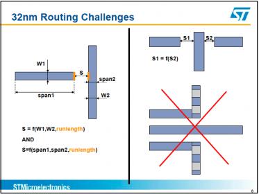
DFM rules at 32nm are a real challenge to P&R tools because of the complexity on what’s acceptable with metal spacing:
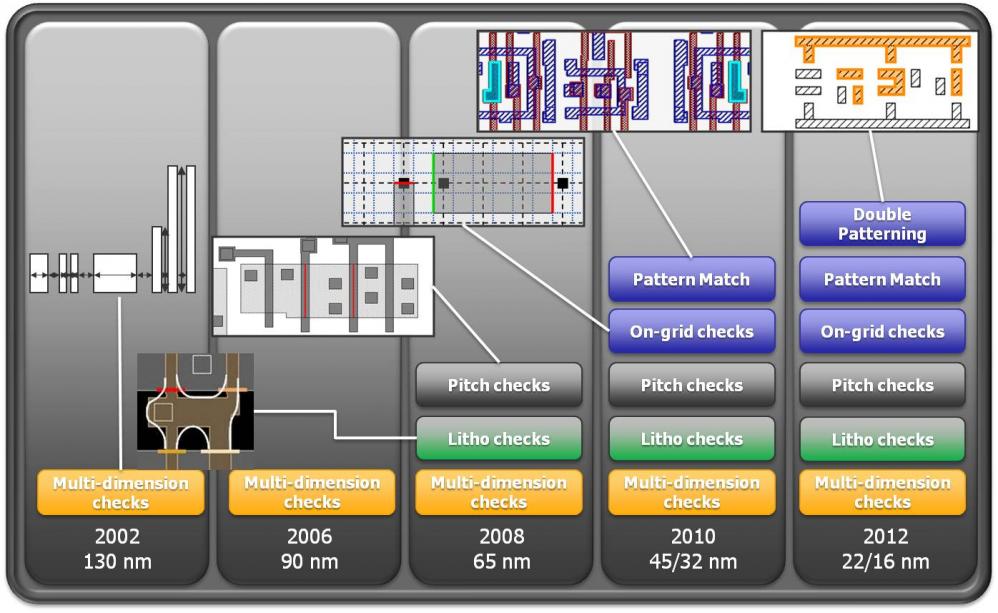
Increasing DRC Complexity is causing more steps at the foundry to ensure yield:
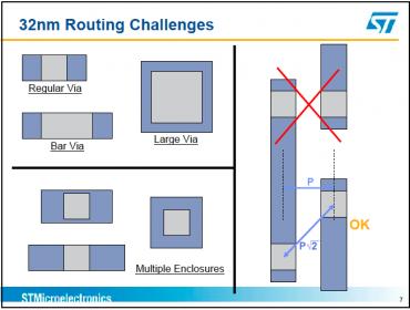
Via rules become an increasing issue:
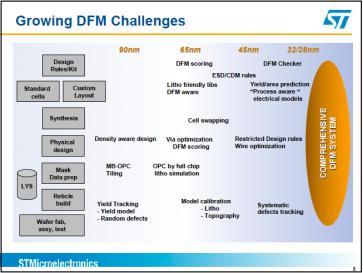
DFM checking is a must at 32/28nm:
The old sign-off flows are taking too much time because of too many violations:
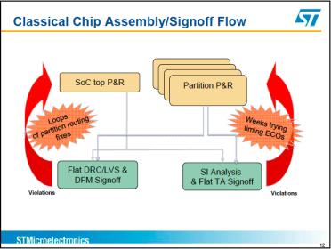
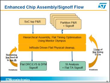
The approach at Mentor to change these violation iterations is a P&R tool with Calibre inside that finds and fixes DFM issues in a preventive mode:
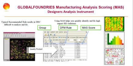
Global Foundries is using DRC+ which adds pattern matching to the approach of design rule checking, once again using the Calibre tool.
The Mentor P&R tool is called Olympus and as it uses Calibre they name it InRoute so that any Calibre engine can be used during P&R. This combination allows the IC designer to optimize their design for both ground rules and recommended rules.
Global Foundries can run a DRC on your IC layout and then use a Manufacturing Analysis Scoring (MAS) to give a quantitative estimate of impact for any DFM violation.
What impressed me was to hear that even the billion transistor graphics chips from Nvidia can be run thru Mentor’s P&R tool when connected with Calibre.
Conlusions
I’m seeing that Mentor has a complete tape-out flow now at 28nm, not just a few point tools. I know that ST is the leading customer using Olmpus with Calibre, so I would expect more customer tape-out stories to surface in 2011.


Comments
0 Replies to “Getting to the 32nm/28nm Common Platform node with Mentor IC Tools”
You must register or log in to view/post comments.