You are currently viewing SemiWiki as a guest which gives you limited access to the site. To view blog comments and experience other SemiWiki features you must be a registered member. Registration is fast, simple, and absolutely free so please,
join our community today!
Translating Intelby Scotten Jones on 01-28-2015 at 10:00 pmCategories: Foundries
Some of Intel’s technology posts make some pretty specific statements and I have seen a number of posts where people seem to have misinterpreted what Intel was actually saying.
Multi Patterning
I have seen a lot of confusion on this one with some people saying Intel didn’t use multi patterning at 22nm and others saying Intel used … Read More
At major EDA events, CEDA (the IEEE council on EDA, I guess you already know what that bit stands for) hosts a lunch and presentation for attendees and others. This week was ICCAD and the speaker was Lars Liebmann of IBM on The Escalating Design Impact of Resolution-Challenged Lithography. Lars decided to give us a whirlwind tour … Read More
Intro
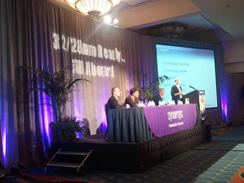
The 28nm nodes is ready with foundry silicon, IP and EDA tools. Tuesday morning at the DAC breakfast I learned more about the 28nm eco-system.
Notes
Why 32/28nm
–Lower power, high integration requirements, mobile applications
What is Ready?
–IP is qualified (ARM, Memories, Foundation IP, SNPS IP, PDKs)
–… Read More
Last week I talked with two experts at Mentor about the challenges of getting IC designs into the 32nm/28nm node on the Common Platform (IBM, GLOBALFOUNDRIES and Samsung). Global Foundries issued a press release talking about how the four major EDA companies have worked together to qualify EDA tools for this node.
Sudhakar Jilla,… Read More


