Interconnect plays a significant role in the semiconductor design of a SoC; if not architected and handled well, it can lead to an overdesigned SoC impacting on its power, performance and area. Since a SoC generally contains multiple IPs requiring different data paths to satisfy varying latency and performance cycles, it has become extremely difficult to architect an interconnection for the overall SoC which can provide the best throughput as well as latency. A single cycle mismatch can lead the interconnect fabric to allow low priority traffic and block high priority traffic. A load-balancing is extremely important for high performance on critical paths and management of traffic for less performance intensive slower paths. For example, the bus fabric between CPU and main memory, through memory controller, must be configured such that the memory bandwidth is maximized whereas latency is minimized.
The problem doesn’t end with a good optimized architecture; the real challenge comes when performance critical paths need fine tuning in the real design and that gets prohibited by the architecture. So, what’s the way out? I’m delighted to see a novel approach provided by Carbonthrough its state-of-the-art Virtual Prototyping tool, SoC Designer. It progressively balances architectural optimizations with real accurate performances as and when the design decisions are made down the cycle of the overall SoC design.
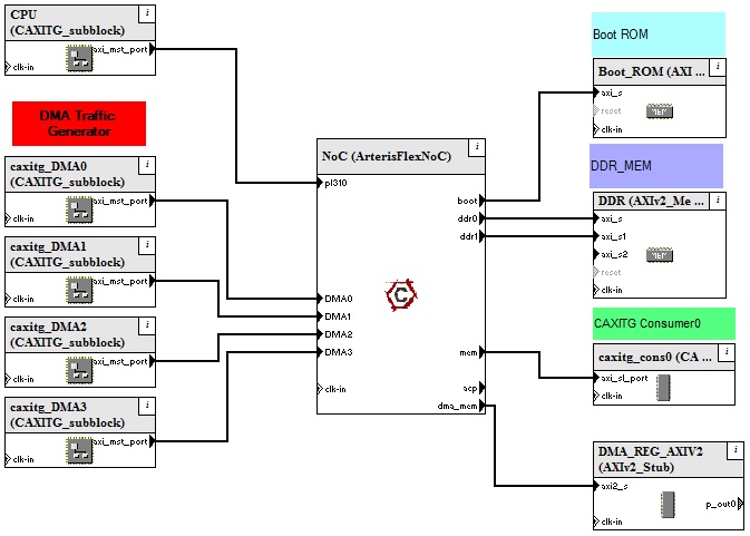
[Architectural Exploration – CAXITG and Memory models connected through Arteris FlexNoC]
It’s a two phase approach. In the first phase (i.e. architectural exploration), Carbon IP Exchange is used to configure 100% cycle accurate interconnect model and quickly isolate performance bottlenecks with traffic generators and flexible memory sub-systems. Above picture shows how Carbon AXI Traffic Generator (CAXITG) and memory models are configured with 100% cycle accurate Arteris FlexNoCinterconnect. CAXITG enables performance analysis of AMBA AXI-based systems in Carbon SoC Designer. Traffic such as read/write, pipelining, random data rate, throughput and latency can be profiled. Transaction tracing and back-pressure analysis can be done. Waveforms can be viewed within SoC Designer to identify performance bottlenecks. Wait states can be used to simulate low performing memory sub-systems. Cost Vs performance trade-off analysis can be done for the interconnect fabric. It’s wise to use bandwidth and latency as required to conserve power.
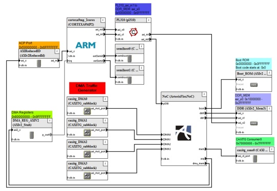
[Arteris FlexNoC with ARM Cortex A9 dual core CPU]
The second phase involves optimizing the system with real implementation accurate IP blocks and real world workloads. Virtual Prototypes allow this reusability with great ease. Above is an example where the traffic generator has been replaced with an ARM Cortex A9 processor. Design trade-offs can be re-visited and re-validated against actual multicore processor traffic. Similarly, the platform can be further updated with actual DMA and memory controller IPs.
Another complexity in interconnect optimization comes from hardware based cache coherency. AXI Coherency Extensions (ACE) to AMBA bus protocols introduce extra complexity of commands complying with ACE specifications, maintaining cache state to ensure coherency and legality operations and correct execution of Barrier transactions across multiple cores issuing such transactions.
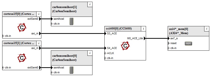
[Carbon A15 bare metal CPAK multi-processor reference platform]
The A15 Bare Metal CPAK can be used very effectively to analyse cache coherency and its performance implications with an ARM Cortex A15 and ARM CCI-400 Cache-Coherent Interconnect.
SoC Designer has in-built ACE monitoring capabilities. A comparison of non-coherent and coherent workloads can be made instantly.
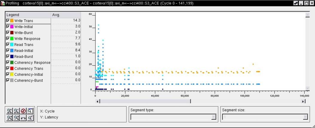
[Non-coherent A15 application workload – Average read latency ~9.6 cycles]
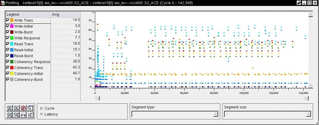
[Coherent A15 workload (same application) – Average read latency ~16.5 cycles]
The SoC Designer profiling helps quantify the cost of coherency in the broader context of overall system performance. This can also provide clear understanding of design partitioning across multiple networks on chip.
A detailed description of various capabilities of SoC Designer and procedures for performance optimization of interconnect for SoC design without wasting power or area is given in a whitepaperat Carbon website. It’s worth reading and knowing about what this Virtual Prototyping platform can do for you.
More Articles by Pawan Fangaria…..
lang: en_US
Share this post via:


Silicon Insurance: Why eFPGA is Cheaper Than a Respin — and Why It Matters in the Intel 18A Era