

The semiconductor industry today is faced with several substantial issues—the continuing rise in design costs for complex SoCs, the decrease in the incidence of first-time-right designs and the increase in the design cycle time against shrinking market windows and decreasing product life cycles. An additional factor has now been added to SoC design costs with the emergence of complicated software applications intended to run on the SoC silicon. The costs of the software effort have outstripped the silicon design costs and have become the major part of the cost of these designs. IP integration is also a growing part of design costs.

As happens often in our industry, the right solution surfaces at the right time. That solution is the incorporation of AI functionality into existing EDA tools as an aid to silicon and software designers and to make these designers more efficient and productive. While these tools will not solve every problem, they will allow for reasonable reductions in design costs and design cycle times. These improvements, by themselves, make the investments in these tools worthwhile and can immediately be impactful to the bottom lines of most companies.
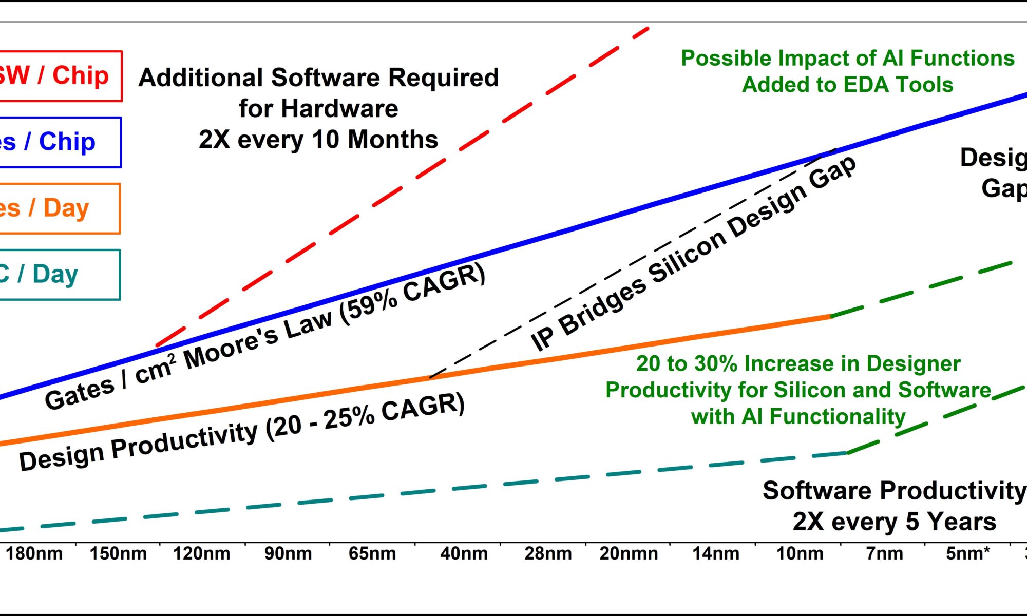
The use of EDA tools with AI functionality can greatly alter the trajectory of the design effort and later, the introduction to the market of products designed with these tools.
The current trend in the EDA market for tools with AI functionality is to make designers more productive and efficient, acting as aids in the design process. A possibility for the future through the continuous learning capabilities of AI is to make suggestions to designers on better methods of doing their designs. The aim here is not to replace the designer, but to improve and expand the capabilities and expertise of the designers. This trend will also extend to the writing of the software applications that accompany the silicon solution. ‘Human-in-the-Loop’ is going to be trend for many years to come.
Decreased design cycle times and reduced design costs may prompt some companies to undertake more designs in the same time they had done only one or two before. While this may be possible, overall market conditions and requirements will ultimately dictate the behavior of companies in this area. In certain instances, a market share battle between competitors may ensue, but will be ill-advised if not managed correctly.
Currently AI functionality is being added to EDA tools in the form of add-on modules. This is both the fastest and most cost-effective method of deploying these capabilities in the short term. The idea is to make the existing tools better with the least amount of disruption. However, Semico believes this will be temporary. We believe that most companies will eventually re-architect their tools to incorporate the AI functionality as a standard feature. It is difficult to imagine any designer not wanting to use tools that are more efficient, faster, more accurate and deliver more cost-effective solutions. No doubt, marketing departments will be working overtime to determine what works and what doesn’t. What customers do and don’t want as part of the tools to incorporate into their deign flows. This will take some time to ascertain and efforts to build the tools from the ground up, incorporating AI functionality as standard features will then follow quickly. Until then, the add-on module approach would seem to be the most effective and economical.
Semico is currently forecasting that the penetration rate for AI-enabled EDA tools will be at least 47.8% by 2025. This rate could be higher but will be gated by several factors:
- Tool cost and availability from major vendors
- Compatibility with existing tools
- Breadth of coverage of different aspects of the design flow
- Efficiency and Efficacy
Our view is that the introduction of AI-enabled EDA tools represents a leap forward in semiconductor design solutions and technology. In a typically semiconductor industry-focused approach, we are going to use a newer technology – AI enabled EDA tools, to solve another persistent problem caused by technology – rising device complexity levels causing escalating design costs and increasing design cycle times.
Finally, Semico believes that the future is bright for companies that can deliver the right solutions at the right time and AI-focused EDA tools enable this goal brilliantly.
Semico has recently written a report covering this topic; New Directions in the EDA Market: Designing with AI Tools, SC109-20 October, 2020
Here is a link to the Table of Contents on our website: https://semico.com/content/new-directions-eda-market-designing-ai-tools
Share this post via:


Intel 18A vs Intel 18A-P: What Is the Difference and Why Does It Matter?