This week, I had a nice opportunity meeting Charu Puri, Corporate Marketing and Sushil Gupta, V.P. & Managing Director at Atrenta, Noida. Well, I know Sushil since 1990s; in fact, he was my manager at one point of time during my job earlier than Cadence. He leads this large R&D development centre, consisting about 200 people at Atrenta’s Noida facility. In fact, they have just moved into a new building, yet to be inaugurated. I will write more about it and various development stories when the inauguration happens.

[Sushil Gupta]
Coming back to Atrenta’s product and technology edge; it was an intriguing discussion on how Atrenta is solving today’s SoC problems. Sushil talked about Atrenta’s SpyGlass being deployed for SoC designs across the complete mobile ecosystem; rightly, as what we have on a PC or laptop today has shifted to the handheld smart phone. And that has been possible with the advent of SoCs where multiple functionalities have been squeezed into the same chip. However it’s not so simple a road to ride as there are tremendous challenges considering the very small window of opportunity for a design, the complexities of verifying and integrating multiple blocks and IPs from different origins, process bottlenecks and physical effects at small geometries, performance-power-area optimization and so on. The only viable option is to reduce long iterative loops in the design flow and introduce shorter and faster loops, early in the cycle, to set the design right. That would significantly reduce the possibility of re-spins and also provide an edge for time-to-market.
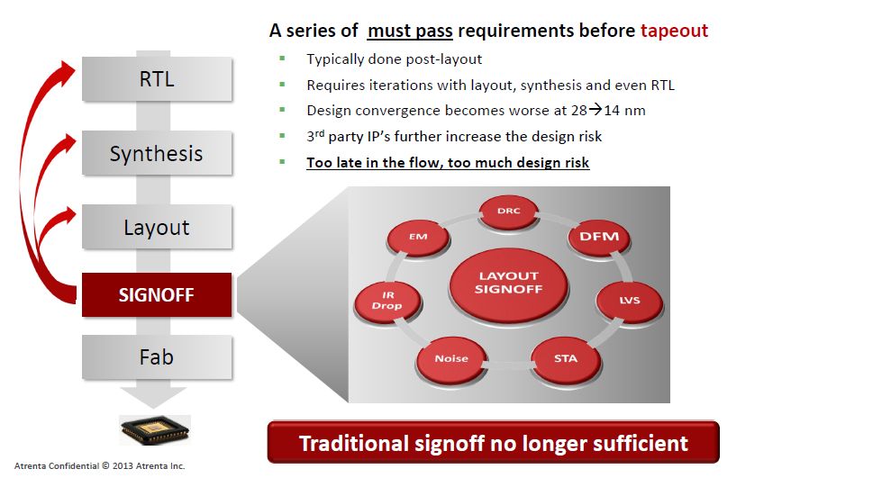
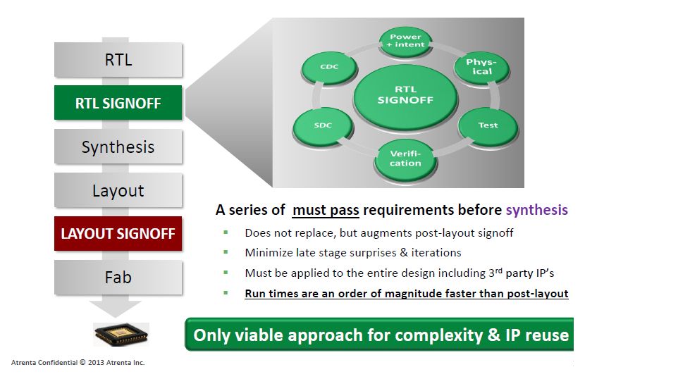
So, there comes Atrenta’s philosophy of pulling up the sign-off process at the earliest possible opportunity, i.e. at the register transfer level (RTL). Well, that cannot completely eliminate layout sign-off, however can definitely and significantly reduce long iterative loops from layout to earlier stages and enable the designer to achieve faster convergence of the design. Traditionally, sign-off is done at the last stage prior to fab, i.e. layout.

As is evident, post layout sign-off is too late and too risky.

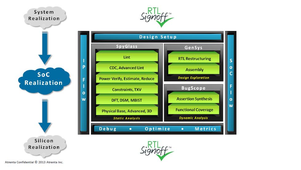
Atrenta’s guiding methodology is to do RTL sign-off before proceeding further. And Atrenta provides a complete platform for RTL sign-off. That’s amazing!!

As we can see, the platform contains all the ingredients to realise an SoC that includes a complete design flow, IP flow and integration, debug and optimization. In fact, Atrenta has also collaborated with TSMCand provides an IP Kit which validates and qualifies any soft IP as per TSMC process before they are integrated into SoCs.
I will talk more about Atrenta’s individual products/technologies and their capabilities in my future articles. But I must share my remembrance that when I had a first read (about two years ago) of the Atrenta SoC Realization whitepaper, I had talked about it with Sushil in his earlier office. And today, to my excitement, Atrenta has really further strengthened that realization!!
Share this post via:


Agentic AI Demands More Than GPUs