Yesterday at SEMICON West I attended an interesting talk about how to use the masses of die test data to improve silicon yield. The speaker was Dr. Martin Keim, from Mentor Graphics.
First of all, he pointed out that with advanced process nodes (45nm, 32nm, and 28nm), and new technologies like FinFETs, we get design-sensitive defects. This means that even when the design passes DFM/DRC, there are some design patterns that fail. The normal way to find these is through physical failure analysis (PFA to the cool kids); after the silicon is fabricated, wafer test finds defective parts, and the product engineers decide which of those parts to cut open and inspect. They are looking for the root cause of the failure to feed back into the design process. The decisions they make for PFA are based on test data. And there is a lot of it. However PFA alone can’t explain the root cause for layout pattern induced defects. The smaller feature sizes and new device structures of technologies like 14nm and FinFET introduce additional challenges.
The trick then, is to harness, sort, and present this failure data in a way that saves time and money and moves the whole world forward. It’s useful, Keim says, to correlate this physical fail data to the layout, and to DFM rules. That makes the results actionable. It’s then essential, he continued, to filter out the noise. With a lot of data, comes a lot of noise.
So, here’s what he showed suggests:
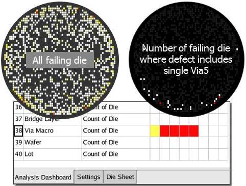
“Test fail data contains a goldmine of information.” This picture shows how the fail data is used to find the location of defect in the layout and what kind of defect it is. This makes more failed die suitable for PFA because they now know exactly where to look for the defect. It also uncovers systematic defects; information that feeds back to manufacturing and design in order to improve yield quickly.
Next, he explained how this same data can find critical design features.
Say PFA finds the root cause shown on the upper right. What does this tell you about the very similar patterns on the bottom? Do those also fail? You can get that answer. “It’s all in the data,” says Keim. You simply combine the output from layout-aware diagnosis (the suspect defects on top right) and the results of your DFM analysis. The DFM rule violation becomes a property of the diagnosis suspect. With statistical analysis, you can then determine the root cause pattern and, this is key, evaluate potential fixes. That last part is important because you can get immediate feedback on how to fix that defect before you go through another round of silicon. Keim stressed how important it is to be able to validate a proposed fix to the observed current defect. This validation will tell you if the proposed fix actually will have an impact on the current problem without screwing up things elsewhere.
He noted that for FinFETS, we need transistor-level diagnosis to find the potential defect mechanisms within the transistor itself. He says that their early research shows good correlation between where the diagnosis results say a defect is and where PFA actually finds it. To bring this to the full potential, effective transistor-level ATPG is a valuable asset, says Keim.
His final point about all the test data was about all the noise. Ambiguity isn’t helpful, he said definitively. To deal with the noise, Mentor has an algorithm they are calling “root cause deconvolution.”
Convoluted, adjective, meaning involved, intricate. A convoluted explanation leaves you more confused. A convoluted hallway leaves you lost. Convoluted test data leaves you with murky conclusions. Presumably, deconvolution (don’t look for it in Merriam-Webster), clarifies the root cause of the failure from the giant, smelly swamp of raw test data. This nifty technique eliminates the noise.
These powerful ways of using test data promises to accelerate the time it takes to find the root cause of chip failures that limit yield, and thus to improve yield ramp. Because product cycles are now shorter than process technology cycles, a fast yield ramp is a key component of success in the market.
For your viewing enjoyment, and for an in-depth look at yield improvement, Mentor offers this on-demand webinar “Accelerating Yield and Failure Analysis with Diagnosis.”
Share this post via:


Silicon Insurance: Why eFPGA is Cheaper Than a Respin — and Why It Matters in the Intel 18A Era