IC designers of passive devices often use empirical approaches to perform High Frequency Analysis (HFA), however there is at least one new approach being offered by Mentor Graphics using a tool flow of:
- Device detection and extraction with Calibre LVS and Calibre PERC
- Interconnect RLC extraction with Calibre xRC, Calibre xACT-3D and Calibre xL
- 3D-IC design rule checking with Calibre 3DSTACK
- Design environment integration with Calibre Interactive
A recent White Paper was written by Georgios Manetas, Ph.D, Developer and Christen Decoin, Program Manager. I’ll give you an overview from what I read.

Empirical Approach
You could first design multiple silicon test structures for HF devices, create a compact model with TCAD tools and then calibrate the models. Some reasons that make the empirical approach less appealing:
- Long development time for TCAD models
- Measurement-based design takes too much time
- Small changes to the passive device design require new models
- Parasitic and neighboring device interactions are not accounted for
- It’s difficult to perform design explorations
Mentor’s Approach
In the opening paragraph I listed all of the Mentor tools used to perform HFA of passives, and here are how the tools would be used:
- Inductor devices are automatically recognized in the IC layout with either Calibre nmLVS-H or Calibre xRC.
- Electro-Magnetic (EM) simulation with Calibre xACT-3D, producing S-parameters which are frequency dependent.
Accuracy versus Reference
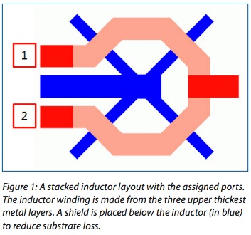
New approaches must be compared against a reference, so the inductor layout from Figure 1 was used and the two approaches compared. The Mentor S-parameters are within 5% of the reference (TCAD-based) L values, and within 10% of Q values:


Benefits of New Approach
So the accuracy of the new approach looks acceptable, other benefits include:
- Scalable tool flow, about 10X capacity and performance improvement over TCAD tools
- Enables device exploration, quickly
- Tools integrated with full-custom layout editors
- Analyze with black-boxing to exclude areas
- Extract and analyze in hours, not days
- Characterize both HF components and the IC interconnect
- At validation stage use highest accuracy with good turn around time
- For design exploration use good accuracy and fast turn around time
Summary
HF designers now have another choice besides a traditional TCAD approach by using Mentor tools. The complete white paper can be found here.
Further Reading
- Automating Complex Circuit Checking Tasks
- Measuring the Accuracy of a 3D Field Solver for IC Extraction
- Who Needs a 3D Field Solver for IC Design?
- An Affordable 3D Field Solver at DAC
- Memory Cell Characterization with a Fast 3D Field Solver
- A New Hierarchical 3D Field Solver
- Nimbic (formerly Physware) – 3D Field Solver in the Cloud or Desktop
- QuickCap for IC Extraction at DAC 2011
- 3D Transistors and IC Extraction Tools
- How Do You Extract 3D IC Structures?
- TSMC Theater Presentation: Lorentz Solution!
- Nimbic (formerly Physware) – 3D Field Solver in the Cloud or Desktop
- Why X-Fab uses 3D Resistance Extraction and Analysis
- Advanced Memory Cell Characterization with Calibre xACT 3D
- Reducing the Need for Guardbanding Flash ADC Designs


Comments
There are no comments yet.
You must register or log in to view/post comments.