Always in motion is the future. ~Yoda
For nearly ten years now, full-chip simulation engines have successfully used process models to perform OPC in production. New full-chip models were regularly introduced as patterning processes evolved to span immersion exposure, bilayer resists, phase shift masking, pixelated illumination sources, and much more. The models, in other words, have kept up with and enabled the relentless march into the lithographic nanosphere.[SUP]1
[/SUP]
“Hello? 1983 calling.” Perhaps this is what Yoda was talking about—technology such as this Motorola DynaTAC 8000x ushered in the age of microelectronics.
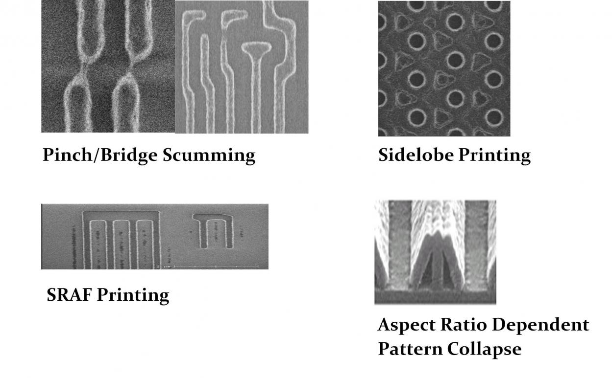
We learned from Yoda that the future is not set, it is always in motion. Still, I feel confident that the industry can predict several areas where full-chip models will need to evolve and improve.[SUP]2[/SUP] As process margins continue to narrow at lower k[SUB]1[/SUB], models will need to more faithfully predict all failure modes which loiter at the process window corners. In addition to pinching and bridging, models will need to accurately predict behaviors you may be less familiar with: sub-resolution assist feature (SRAF) scumming / dimpling, side-lobe dimpling, and aspect ratio induced mechanical pattern collapse (Figure 1). These can all lead to defects in the etched layer.
Figure 1. Emerging patterning failure modes.
While full-chip OPC models based on a 2D contour simulation have so far been sufficient to meet the task of correction and verification, we may need some 3D awareness in these models. For example, we might need to account for underlying pattern topography/reflectivity for implant layer patterning, or want an etch model to predict bias as a function of lithographic focus (which imparts resist profile changes). One thing to be certain of – 3D mask topography effects will continue as target and SRAF dimensions shrink, and improvements in the accuracy of 3D mask models must keep pace.
Another emerging technology, Source Mask Optimization (SMO), may place greater demands upon the portability of process models. With SMO, the illumination source is dynamically changed on a design-by-design basis in manufacturing, yet a single calibrated resist model is preferred for optimum cycle time. Full-chip mask process models may be needed to facilitate portability, and to enable maximum flexibility for process evolution.
New processes are emerging for double patterning including litho-etch-litho-etch and litho-freeze-litho-etch, sidewall image transfer, and negative tone develop. Novel chemical and thermal pattern shrink processes will continue to find their way into manufacturing. These processes represent a wide range of complex physiochemical processes, but the phenomenological compact model approach, based upon relatively few optical parameter inputs, and empirical CD/contour outputs, will no doubt be able to accurately represent these processes for full-chip simulation.
Finally, another emerging process is EUV lithography. In order to accurately perform full-chip simulation, optical models that account for flare and field-dependent mask shadowing will be required. These models are already in mature development. It is important to highlight that “OPC” will indeed be required for EUV, despite the fact that the lower wavelength will deliver a substantially higher k[SUB]1[/SUB] factor than 193 nm lithography.
Model accuracy and predictive capability requirements will surely continue to shrink below today’s 1.0 nm, and additional requirements beyond simple single-plane CD will be required. Perhaps it’s time to increase our accuracy budget 10X by converting to units of Angstroms—it will make us feel like there is more room at the bottom of the scaling curve!
As a final note, the SPIE Advanced Lithography meeting in San Jose (12-16 February) has an ever-expanding conference focused on design for manufacturability through design-process integration. As the co-chair of this conference, I can say with certainty that the technical presentations are of the highest quality. If you want to engage more deeply in the interface between IC design and manufacturing, attend the keynotes, papers presentations, and poster session on Wednesday, 15 February, and the joint optical microlithography/DFM joint sessions on Thursday, 16 February.
— John Sturtevant, Mentor Graphics
1—Lots of interesting information about process models in my previous posts: Part I, Part II, Part III, and Part IV.
2—This series was inspired by this paper I presented at SPIE Advanced Lithography in 2011.
Share this post via:


Comments
There are no comments yet.
You must register or log in to view/post comments.