You are currently viewing SemiWiki as a guest which gives you limited access to the site. To view blog comments and experience other SemiWiki features you must be a registered member. Registration is fast, simple, and absolutely free so please,
join our community today!
WP_Term Object
(
    [term_id] => 386
    [name] => Semiconductor Services
    [slug] => semiconductor-services
    [term_group] => 0
    [term_taxonomy_id] => 386
    [taxonomy] => category
    [description] =>
    [parent] => 0
    [count] => 1190
    [filter] => raw
    [cat_ID] => 386
    [category_count] => 1190
    [category_description] =>
    [cat_name] => Semiconductor Services
    [category_nicename] => semiconductor-services
    [category_parent] => 0
    [is_post] =>
)
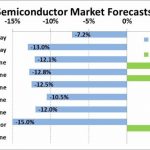
The global semiconductor market is headed for a double-digit decline for the year 2019 after a decline of 15.6% in first quarter 2019 from fourth quarter 2018. According to WSTS (World Semiconductor Trade Statistics) data, this was the largest quarter-to-quarter decline since a 16.3% decline in first quarter 2009, ten years … Read More
At the SPIE Advanced Lithography Conference Imec presented several design papers and I have had the opportunity to review the papers and speak with the authors. In this summary I am going to address three emerging areas in order of when I think they may be implemented from soonest to latest.
Specifically, I will discuss:
- Buried Power
…
Read More
2020 capex likely down at least 20% vs 2019 DRAM & NAND price drops versus slowing capacity. Investors happy cause it could have been worse.
Micron reported $1.05 in Non-GAAP EPS beating street consensus of $0.79 by $0.26. While this looks like a big beat, we would remind investors that estimates for the quarter were about… Read More
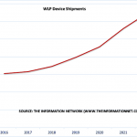
Advanced IC packaging, such as fan-out WLP (Wafer Level Packaging) and 2.5D TSV (Through Silicon Via) will drive the packaging equipment market, particularly lithography. This will help specific equipment manufacturers in 2019, since the WFE (Wafer Front End) market will drop 17%. But the Back-End lithography market, led … Read More
SEMICON West and ES Design West are right around the corner here in San Francisco and I wanted to point out the Meet the Experts segment in the appropriately named Meet the Experts Theater. Great idea really and a super great line-up. The best part of course is actually meeting the experts. Over my 35 year semiconductor career I have… Read More
The good news is that the next five DAC events will take place in Moscone Center in San Francisco! If going to Las Vegas from the Bay area is an easy trip, coming from Europe to Las Vegas makes it a 24+hours journey… One obvious consequence was the poor attendance to the exhibition floor. But let’s be positive and notice that the number… Read More
eSilicon was one of the first companies to focus on making the benefits of the fabless semiconductor movement available to a broader range of customers and markets. The company is credited with the creation of the fabless ASIC model. In this section, eSilicon shares some of its history and provides its view of the ever-changing … Read More
We had warned in our May 10th note about the rare earth element risk. It is one of the few remaining leverage points that China has left that has a potentially strong impact on the US much similar to the US’s impact on Huawei and perhaps even worse. Cutting the US off from rare earth elements is clearly worse than cutting Huawei
…
Read More
Semiconductor chip package technologies have evolved throughout the years to the point where hundreds of package types are available today.
Most applications will require the more general, single-element packaging for integrated circuits and the other components such as resistors, capacitators, antenna etc. However,… Read More
Every morning I read the headlines from SemiWiki, CNN, LinkedIn and my Twitter feed, and it seems like every week that I read about another security breach that makes me wonder if anything online is secure. Companies try to harden their web sites, IT infrastructure and even their electronic products from being exploited or tampered… Read More


Silicon Insurance: Why eFPGA is Cheaper Than a Respin — and Why It Matters in the Intel 18A Era