You are currently viewing SemiWiki as a guest which gives you limited access to the site. To view blog comments and experience other SemiWiki features you must be a registered member. Registration is fast, simple, and absolutely free so please,
join our community today!
WP_Term Object
(
    [term_id] => 386
    [name] => Semiconductor Services
    [slug] => semiconductor-services
    [term_group] => 0
    [term_taxonomy_id] => 386
    [taxonomy] => category
    [description] =>
    [parent] => 0
    [count] => 1220
    [filter] => raw
    [cat_ID] => 386
    [category_count] => 1220
    [category_description] =>
    [cat_name] => Semiconductor Services
    [category_nicename] => semiconductor-services
    [category_parent] => 0
    [is_post] =>
)
Ollie Jones, Vice President of Strategic Sales at Sondrel, has worked extensively across Europe, North America and Asia and has held a variety of commercial leadership roles in FTSE 100, private equity owned and start-up companies.
Most recently Ollie was Chief Commercial Officer for an EV battery start up where he led the acquisition… Read More
From humble beginnings in military applications, the semiconductor industry has been fundamental to all societal growth, and everything that grows exponentially depends on semiconductors.
It is not a gentle industry. Products over two years old are unsellable, and there is either too much supply or none. Semiconductor scarcity… Read More
224 Gbps PAM4 gets attention for applications such as data center, AI/ML, accelerated computing, instrumentation and test and measurement. The question is how real is it and what are the challenges that need to be overcome to implement reliable channels at that data rate? If you wonder about these kinds of topics for your next design,… Read More
The performance demands of data centers continue to grow, driven to large degree by the ubiquitous use of complex AI algorithms. On April 25, Embedded Computing Design held an informative webinar on this topic. Two experts looked at the problem from the standpoint of processor architecture and communication strategies, which… Read More
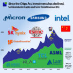
We are in the semiconductor market phase where everybody disagrees on what is going on. The market is up; the market is down. Mobile phones are up…. oh no, now they are down. The PC market is up—oh no, we need to wait until we can get an AI PC. The inflation is high—the consumer is not buying.
For us in the industry, the 13-week financial … Read More
A high-quality verification campaign including methods able to absolutely prove the correctness of critical design behaviors as a complement to mainstream dynamic verification? At first glance this should be a no-brainer. Formal verification offers that option and formal adoption has been growing steadily, now used in around… Read More
– KLA reported a good QTR but more importantly passing the bottom
– Lead times mean KLA gets orders early in up cycle-just behind ASML
– Potential upside in upcycle as packaging needs more process control
– 2024 2nd half weighted with stronger recovery likely in 2025
A solid quarter as expected with good
…
Read More
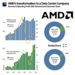
AMD’s Q1-2024 financial results are out, prompting us to delve into the Data Center Processing market. This analysis, usually reserved for us Semiconductor aficionados, has taken on a new dimension. The rise of AI products, now the gold standard for semiconductor companies, has sparked a revolution in the industry, making… Read More
– Lam reports another flat quarter & guide- No recovery in sight yet
– Seems like no expectation of recovery until 2025- Mixed results
– DRAM good- NAND weak- Foundry/Logic mixed-Mature weakening
– Clearly disappointing to investors & stock hoping for a chip recovery
Another Flat Quarter &
…
Read More
On Friday April 12th Intel held a press briefing on their adoption of High NA EUV with Intel fellow and director of lithography Mark Phillips.
In 1976 Intel built Fab 4 in Oregon, the first Intel fab outside of California. With the introduction of 300mm Oregon became the only development site for Intel with large manufacturing, development,… Read More


Consolidation and Competition: Who is Winning the $4.5 Billion Interface IP Race?