You are currently viewing SemiWiki as a guest which gives you limited access to the site. To view blog comments and experience other SemiWiki features you must be a registered member. Registration is fast, simple, and absolutely free so please,
join our community today!
            WP_Term Object
(
    [term_id] => 24
    [name] => TSMC
    [slug] => tsmc
    [term_group] => 0
    [term_taxonomy_id] => 24
    [taxonomy] => category
    [description] =>
    [parent] => 158
    [count] => 621
    [filter] => raw
    [cat_ID] => 24
    [category_count] => 621
    [category_description] =>
    [cat_name] => TSMC
    [category_nicename] => tsmc
    [category_parent] => 158
    [is_post] =>
)

WP_Term Object
(
    [term_id] => 24
    [name] => TSMC
    [slug] => tsmc
    [term_group] => 0
    [term_taxonomy_id] => 24
    [taxonomy] => category
    [description] =>
    [parent] => 158
    [count] => 621
    [filter] => raw
    [cat_ID] => 24
    [category_count] => 621
    [category_description] =>
    [cat_name] => TSMC
    [category_nicename] => tsmc
    [category_parent] => 158
    [is_post] =>
)
The 5[SUP]th[/SUP] annual TSMC OIP Forum was last week and thankfully there were no surprises with the exception of how many people asked me who I think will be the next TSMC CEO. Certainly I have no idea but I would be happy to use my incredible powers of deductive reasoning to determine who it will be.
The TSMC Open Innovation Platform®… Read More
One of TSMC’s two big Silicon Valley events each year is the Open Innovation Platform (OIP) Forum. This year it is on Tuesday October 1st. It is in the San Jose Convention Center and starts at 9am (registration opens at 8am). Pre-registration to attend is now open here or click on the image to the right.
From 9.10 to 9.40 is the … Read More
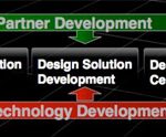
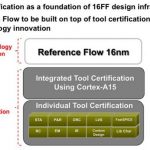
The existence of TSMC’s Open Innovation Platform (OIP) program further sped up disaggregation of the semiconductor supply chain. Partly, this was enabled by the existence of a healthy EDA industry and an increasingly healthy IP industry. As chip designs had grown more complex and entered the system-on-chip (SoC) era, the amount… Read More
Today TSMC announced three reference flows that they have been working on along with various EDA vendors (and ARM and perhaps other IP suppliers). The three new flows are:
- 16FinFET Digital Reference Flow. Obviously this has full support for non-planar FinFET transistors including extraction, quantized pitch placement, low-vdd
…
Read More
Now that the IDF 2013 euphoria is fading I would like to play devil’s advocate and make a case for why Intel is still not ready to compete in the mobile market. It was very clear from the keynotes that Intel is a chip company, always has been, always will be, and that will not get them the market share they need to be relevant in mobile electronics,… Read More
The history of TSMC and its Open Innovation Platform (OIP) is, like almost everything in semiconductors, driven by the economics of semiconductor manufacturing. Of course ICs started 50 years ago at Fairchild (very close to where Google is headquartered today, these things go in circles). The planarization approach, whereby… Read More
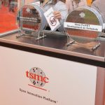
The TSMC Open Innovation Platform® (OIP) Ecosystem Forum brings TSMC’s design ecosystem member companies together to share with our customers real-case solutions for customers’ design challenges and success stories of best practice in TSMC’s design ecosystem.
More than 90% of the attendees last year said “this… Read More
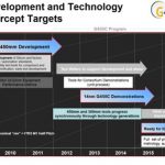
The presentations from the 450mm sessions at SEMICON West are up now. After talking to equipment manufacturers and the foundries I’m fairly confident 450mm wafers will be under our Christmas trees in 2016, absolutely. TSMC just increased CAPEX again and you can be sure 450mm is part of it. SEMI has a 450mm Central landing page HERE… Read More
There is an interesting article on Seeking Alpha, “A More Profitable Semiconductor Company Than Intel”, and for a change the author does not PRETEND to know semiconductor technology. Refreshing! Personally I think the stock market is a racket where insiders profit at the expense of the masses. But if you are going to gamble you … Read More
One of the more interesting pieces of information I overheard at SEMICON West earlier this month was that Intel 14nm was delayed. This rumor came from the semiconductor equipment manufacturers and they would know. What I was told is that the Intel 14nm process has not left the OR development facility to be replicated in the OR and … Read More