You are currently viewing SemiWiki as a guest which gives you limited access to the site. To view blog comments and experience other SemiWiki features you must be a registered member. Registration is fast, simple, and absolutely free so please,
join our community today!
            WP_Term Object
(
    [term_id] => 24
    [name] => TSMC
    [slug] => tsmc
    [term_group] => 0
    [term_taxonomy_id] => 24
    [taxonomy] => category
    [description] =>
    [parent] => 158
    [count] => 621
    [filter] => raw
    [cat_ID] => 24
    [category_count] => 621
    [category_description] =>
    [cat_name] => TSMC
    [category_nicename] => tsmc
    [category_parent] => 158
    [is_post] =>
)

WP_Term Object
(
    [term_id] => 24
    [name] => TSMC
    [slug] => tsmc
    [term_group] => 0
    [term_taxonomy_id] => 24
    [taxonomy] => category
    [description] =>
    [parent] => 158
    [count] => 621
    [filter] => raw
    [cat_ID] => 24
    [category_count] => 621
    [category_description] =>
    [cat_name] => TSMC
    [category_nicename] => tsmc
    [category_parent] => 158
    [is_post] =>
)
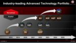
TSMC recently held their annual Technology Symposium in Santa Clara, CA. The presentations provided a comprehensive overview of their status and upcoming roadmap, covering all facets of process technology and advanced packaging development. This article will summarize the highlights of the process technology updates… Read More
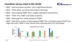
The TSMC Technical Symposium is today so I wanted to give you a brief summary of what was presented. Tom Dillinger will do a more technical review as he has done in the past. I don’t want to steal his thunder but here is what I think are the key takeaways. First a brief history lesson.
The history of TSMC Technology Development with 12 key… Read More
“Inverse lithography technology (ILT) represents the most significant EDA advance in the last two decades.” Danping Peng from TSMC made that assertion at the recent SPIE Advanced Lithography + Patterning Conference, in his talk entitled: ILT for HVM: History, Present, and Future. This article summarizes the highlights… Read More
With the TSMC Technical Symposium coming next month there is quite a bit of excitement inside the fabless semiconductor ecosystem. Not only will TSMC give an update on N3, we should also hear details of the upcoming N2 process.
Hopefully TSMC will again share the number of tape-outs confirmed for their latest process node. Given… Read More
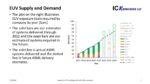
In my “The EUV Divide and Intel Foundry Services” article available here, I discussed the looming EUV shortage. Two days ago, Intel announced their first EUV tool installed at their new Fab 34 in Ireland is a tool they moved from Oregon. This is another indication of the scarcity of EUV tools.
I have been tracking EUV system production… Read More
At the ISS conference held from April 4th through 6th I presented on who I thought would have the leading logic technology in 2025. The following is a write up of that presentation.
ISS was a virtual conference in 2021 and I presented on who currently had logic leadership and declared TSMC the clear leader. Following that conference,… Read More
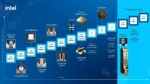
TSMC’s Reliability Ecosystemby Tom Dillinger on 04-06-2022 at 10:00 amCategories: Events, Foundries, TSMC
TSMC has established a leadership position among silicon foundries, based on three foundational principles:
- breadth of technology support
- innovation in technology development
- collaboration with customers
Frequent SemiWiki readers have seen how these concepts have been applied to the fabrication and packaging technology… Read More
The EUV Divide
I was recently updating an analysis I did last year that looked at EUV system supply and demand, while doing this I started thinking about Intel and their Fab portfolio.
If you look at Intel’s history as a microprocessor manufacturer, they are typically ramping up their newest process node (n), in volume production… Read More
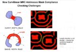
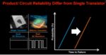
The further scaling of interconnect and via lithography for advanced nodes is challenged by the requirement to provide a process window that supports post-patterning critical dimension variations and mask overlay tolerances. At the recent international Electron Devices Meeting (IEDM) in San Francisco, TSMC presented … Read More
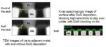
Previous SemiWiki articles have described the evolution of embedded non-volatile memory (eNVM) IP from (charge-based) eFlash technology to alternative (resistive) bitcell devices. (link, link)
The applications for eNVM are vast, and growing. For example, microcontrollers (MCUs) integrate non-volatile memory for … Read More