Tuesday morning at DAC I attended the Synopsys-hosted breakfast to hear from foundries and ARM about the challenges of designing and delivering silicon at the 32nm/28nm and 20nm nodes.
… Read MoreTSMC Theater Presentation: Ciranova!
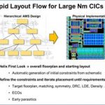
Ciranova presented a hierarchical custom layout flow used on several large advanced-node designs to reduce total layout time by about 50%. Ciranova itself does automated floorplanning and placement software with only limited routing; but since the first two constitute the majority of custom layout time, and strongly influence… Read More
The Black Swan that Catapulted Intel into 2012
Black Swan Events are not to be embraced, they are to be feared, if conventional wisdom holds true. And yet, the 2011 Black Swan that slammed the PC market (i.e. the Thailand Floods that wiped out a large part of the disk drive market) has turned out to be the key catalyst for reshaping the semiconductor industry in 2012 and 2013. Instead… Read More
TSMC Theater Presentation: Atrenta SpyGlass!
Atrenta presented an update on the TSMC Soft IP Alliance Program at TSMC’s theater each day at DAC. Mike Gianfagna, Atrenta VP of Marketing, presented an introduction to SpyGlass, an overview of the program and a progress report. Dan Kochpatcharin, TSMC Deputy Director of IP Portfolio, was also there. Between Mike, Dan, and I there… Read More
BDA TSMC Theater Presentation
I caught the Berkeley Design Automation presentation in the TSMC Theater, where Simon Young (BDA’s director of product marketing) described the Analog FastSPICE (AFS) nanometer circuit verification platform, built on their foundation of very fast, very accurate, high capacity circuit simulation.
BDA claims the AFS platform… Read More
TSMC 28nm is Fabulous! TSM Stock is not so Fabulous!
What a great interview! Xilinx CEO Moshe Gavrielov is right on the money HERE where he credits the high 28nm yields to the “very intimate” linkage in process development with TSMC.… Read More
Collaboration at 28nm, 20nm and 14nm
Wednesday morning I attended a panel discussion with: ARM, IBM, Cadence, GLOBALFOUNDRIES and Samsung.
The panelists all sang the same song of collaboration between EDA, IP and Foundry to enable 28nm, 20nm and even 14nm.… Read More
Understanding and Designing For Variation in GLOBALFOUNDRIES 28nm
On Wednesday there is a User Track Poster Session that examines the design impact of process variation in GLOBALFOUNDRIES 28nm technology. For those of you who are wondering what process variation looks like at 20nm take this 28nm example and multiply it by one hundred (slight exaggeration, maybe).
Variation effects have a significant… Read More
Industry Standard FinFET versus Intel Tri-Gate!
Ever since the “Intel Reinvents Transistors Using New 3-D Structure” PR campaign I have been at odds with them. As technologists, I have nothing but respect for Intel. The Intel PR department, however, quite frankly, is evil. Correct me if I’m wrong here but Intel did not “reinvent” the transistor. Nor did they come up with the name… Read More
GLOBALFOUNDRIES Reference Flows at DAC 2012!
As I mentioned in my blog GlobalFoundries Update 2012, the GFI people are on the move at DAC 2012. Here is a little more detail on the up and coming AMS and Digital reference flows for 28nm and 20nm.… Read More


Musk’s Orbital Compute Vision: TERAFAB and the End of the Terrestrial Data Center