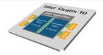
The next generation FPGAs have been announced, and they are BIG! Intel is shipping its Stratix 10 GX 10M FPGA, and Xilinx has announced its VU19P FPGA for general availability in the Fall of next year. The former is expected to support about 80M ASIC gates, and the latter about 50M ASIC gates. And, to bring this mind-boggling gate… Read More

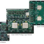
S2C Delivers FPGA Prototyping Solutions with the Industry’s Highest Capacity FPGA from Intel!
In 2016 we published our book “Prototypical: The Emergence of FPGA-Based Prototyping for SoC Design” which began an incredible journey through ASIC prototyping. While we are working on an update to that book there is some recent Prototyping news that is worthy of praise.
First and foremost, S2C Inc. has just announced THE single… Read More
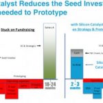
AI Chip Prototyping Plan
I recently had the opportunity to sit down with a chip designer for an AI start-up to talk about using FPGA prototyping as part of a complex silicon verification strategy. Like countless other chip designers for whom simulation alone simply does not provide sufficient verification coverage, this AI start-up also believed that… Read More
WEBNAR: How ASIC/SoC Rapid Prototyping Solutions Can Help You!
If you are considering an FPGA prototype for an ASIC or SoC as part of your verification strategy, which more and more chip designers today are doing to enhance verification coverage of complex designs, please take advantage of this webinar replay:
How ASIC/SoC Prototyping Solutions Can Help You!
Or to get a quick quote from S2C … Read More
Are the 100 Most Promising AI Start-ups Prototyping?
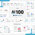
I came across a report on the 100 most promising AI start-ups. The report claimed that CBInsights had “selected the 100 most promising AI start-ups from a pool of 3K+ companies based on several factors …” Wait, what … 3K+ companies!?!? This was a stunning reminder of the sheer magnitude of what is shaping up to be a veritable tsunami… Read More
FPGA Prototyping for AI Product Development

I recently wrote about The Implications of the Rise of AI/ML in the Cloud. In that article, I wrote about my expectation that the rapidly growing AI market will lead to the accelerated use of high-level synthesis (HLS), prototyping, and emulation. In this article, I will focus on the prototyping portion of that – specifically FPGA… Read More
Re Energizing Silicon Innovation
Hardware is roaring back into prominence in technology innovation, from advanced cars to robots, smart homes and smart cities, 5G communication and the burgeoning electronification of industry, medicine and utilities. While software continues to play a role, all of these capabilities depend fundamentally on advances in … Read More
Rapid Prototyping ARM Based Designs Webinar

While writing the definitive book on ARM history we could not have imagined a more different exit than the SoftBank acquisition, not even close. It is now very clear why SoftBank acquired ARM for $31B. It is also very clear why alternatives like RISC-V are trending on SemiWiki and will continue to do so, absolutely. No matter what … Read More
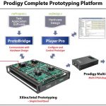
The Importance of Daughter Cards in FPGA Prototyping
FPGA Prototyping started with the advent of FPGAs in the 1980s and today it is a fast growing market segment due to increasing chip and IP complexities up against tightening windows of opportunities. Getting your design verified quickly and allowing hardware and software engineers the opportunity to develop, test, and optimize… Read More
Intel Based FPGA Prototyping Webinar Replay

Due to the overwhelming response, here is the first part of the webinar that I did with S2C and a link to the replay. Richard Chang, Vice President of Engineering at S2C did the technical part of the webinar. Richard has a Masters degree in Electrical engineering from the University at Buffalo and more than 20 years experience designing… Read More