Designers spend plenty of time analyzing the effects of process, voltage and temperature. But everyone knows it’s not enough to simply stop there. Operating environments are tough and have lots of limitations, especially when it comes to power consumption and thermal issues. Thermal protection and even over-voltage protections… Read More
Alchip at TSMC OIP – Reticle Size Design and Chiplet Capabilities
This is another installment covering TSMC’s very popular Open Innovation Platform event (OIP), held on August 25. This event presents a diverse and high-impact series of presentations describing how TSMC’s vast ecosystem collaborates with each other and with TSMC. This presentation is from Alchip, presented by James Huang,… Read More
Highlights of the TSMC Technology Symposium – Part 1
Recently, TSMC held their 26th annual Technology Symposium, which was conducted virtually for the first time. This article is the first of three that attempts to summarize the highlights of the presentations.
This article focuses on the TSMC process technology roadmap, as described by the following executives:
- Y.J. Mii, SVP,
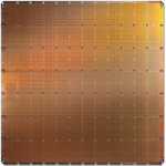
Cerebras and Analog Bits at TSMC OIP – Collaboration on the Largest and Most Powerful AI Chip in the World
This is another installment covering TSMC’s very popular Open Innovation Platform event (OIP), held on August 25. This event presents a diverse and high-impact series of presentations describing how TSMC’s vast ecosystem collaborates with each other and with TSMC. The topic at hand was full of superlatives, which isn’t surprising… Read More
WEBINAR: Addressing Verification Challenges in the Development of Optimized SRAM Solutions with surecore and Mentor Solido
After spending a significant amount of my career in the IP library business it was an easy transition to Solido Design. I spent 10+ years traveling the world with CEO Amit Gupta working with the foundries and their top customers. In fact, the top 40 semiconductor companies use Solido. IP companies are also big Solido users including… Read More
Webinar: Maximize Performance Using FPGAs with PCIe Gen5 Interfaces
FPGAs are a popular method to implement hardware accelerators for applications such as AI/ML, SmartNICs and storage acceleration. PCIe Gen5 is a high bandwidth communication protocol that is a key enabler for this class of applications. Putting all this together presents significant demands on the FPGA for performance and … Read More
Making Full Memory IP Robust During Design
Looking at a typical SoC design today it’s likely to contain a massive amount of memory IP, like: RAM, ROM, register files. Keeping memory close to the CPU makes sense for the lowest latency and highest performance metrics, but what about process variations affecting the memory operation? At the recent DAC conference held… Read More
HCL Webinar Series – HCL Compass Delivers Defect Tracking and More
Similar to my last post on the HCL DevOps webinar series, I will cover their presentation of HCL Compass in a webinar that was recorded on July 29 about how HCL Compass delivers defect tracking and more.
This webinar was presented by Steve Boone, head of product management at HCL Software DevOps, Howie Bernstein, product manager… Read More
ARC Processor Virtual Summit!
The ARC Processor has a rich history. Originally named the Argonaut RISC Processor, it was designed for the Nintendo Game Systems in the 1990s. Argonaut Technologies Limited later became ARC International. My first intimate exposure to ARC was in 2009 when Virage Logic acquired ARC. A year later Virage was acquired by Synopsys… Read More
The Big Three Weigh in on Emulation Best Practices
As software content increases in system-on-chip and system-in-package designs, emulation has become a critical enabling technology for the software team. This technology offers software developers the opportunity to verify their code in against a high-fidelity model of the target system that actually executes fast enough… Read More


The Semiconductor Growth Numbers are Insane but the Real World Doesn’t Tally!