You are currently viewing SemiWiki as a guest which gives you limited access to the site. To view blog comments and experience other SemiWiki features you must be a registered member. Registration is fast, simple, and absolutely free so please,
join our community today!
WP_Term Object
(
    [term_id] => 50
    [name] => Events
    [slug] => events
    [term_group] => 0
    [term_taxonomy_id] => 50
    [taxonomy] => category
    [description] =>
    [parent] => 0
    [count] => 1564
    [filter] => raw
    [cat_ID] => 50
    [category_count] => 1564
    [category_description] =>
    [cat_name] => Events
    [category_nicename] => events
    [category_parent] => 0
    [is_post] =>
)
Everyone knows IP is an important asset for the enterprise. You spend a lot of money on IP licenses. You try to keep track of who bought what as buying the same thing twice is painful. You wonder if you have the latest version of an IP, especially if it’s part of mission-critical functionality. If you’re a good corporate citizen, you … Read More
DesignCon has grown over the years to become a true system design show. The show’s tagline is WHERE THE CHIP MEETS TO BOARD. This is just the beginning. Besides the chip and the board there are all the challenges, opportunities, and options to get signals reliably propagated throughout the entire system. Power, signal integrity,… Read More
The 32nd VLSI Design/CAD Symposium just occurred in a virtual setting. The theme of the event this year was “ICs Powering Smart Life Innovation”. There were many excellent presentations across analog & RF, EDA & testing, digital & system, and emerging technology. There were also some excellent keynotes, and this… Read More
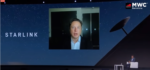
A few weeks ago Mobile World Congress included among its keynotes a live interview with Tesla CEO Elon Musk moderated by Mobile World Live Publisher Justin Springham. The subject was Starlink, the low earth orbit (LEO) constellation intended to deliver global Internet access.
Mobile World Congress Musk keynote interview
Tongue-in-cheek… Read More
Introduction
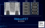
Intel recently provided a detailed silicon process and advanced packaging technology roadmap presentation, entitled “Intel Accelerated”. The roadmap timeline extended out to 2024, with discussions of Intel client, data center, and GPU product releases, and especially, the underlying technologies to be … Read More
Intel presented yesterday on their plans for process technology and packaging over the next several years. This was the most detailed roadmap Intel has ever laid out. In this write up I will analyze Intel’s process announcement and how they match up with their competitors.
10nm Super Fin (SF)
10nm is now in volume production in three… Read More
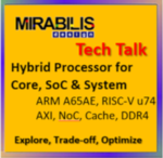
80% of specification optimization and almost 100% of the performance/power trade-offs can be achieved during architecture exploration of product design. RISC-V offers a huge opportunity with lots of pipeline and instruction set enhancement opportunities. Can it really attain the utopian success that people are looking… Read More
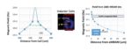
Previous SemiWiki articles have discussed the introduction of embedded Spin-Transfer Torque Magnetoresistive RAM IP from GLOBALFOUNDRIES, as an evolution replacement for non-volatile embedded flash memory. (link, link)
Those articles described the key features of STT-MRAM technology, but didn’t delve into a key reliability… Read More
I had the opportunity to speak with Pete Rodriguez and Alain Labat in regards to the upcoming webinar on M&A. I have worked with both Pete and Alain in the past so I can tell you personally that this event will be well worth your time. This is truly an all star cast with a collective experience base with billions of dollars worth of … Read More
EDA Flows for 3D Die Integrationby Tom Dillinger on 07-20-2021 at 6:00 amCategories: Cadence, EDA, Events
Background
The emergence of 2.5D heterogeneous die integration using a silicon (or organic) interposer has enabled unique system architectures. The term “More than Moore” has been used to describe the circuit density and cost advantages of leveraging multiple die in the package, the die potentially in different process technologies. … Read More


TSMC CoWoS versus Intel EMIB Semiconductor Packaging