You are currently viewing SemiWiki as a guest which gives you limited access to the site. To view blog comments and experience other SemiWiki features you must be a registered member. Registration is fast, simple, and absolutely free so please,
join our community today!
            WP_Term Object
(
    [term_id] => 159
    [name] => Siemens EDA
    [slug] => siemens-eda
    [term_group] => 0
    [term_taxonomy_id] => 159
    [taxonomy] => category
    [description] =>
    [parent] => 157
    [count] => 842
    [filter] => raw
    [cat_ID] => 159
    [category_count] => 842
    [category_description] =>
    [cat_name] => Siemens EDA
    [category_nicename] => siemens-eda
    [category_parent] => 157
    [is_post] =>
)

WP_Term Object
(
    [term_id] => 159
    [name] => Siemens EDA
    [slug] => siemens-eda
    [term_group] => 0
    [term_taxonomy_id] => 159
    [taxonomy] => category
    [description] =>
    [parent] => 157
    [count] => 842
    [filter] => raw
    [cat_ID] => 159
    [category_count] => 842
    [category_description] =>
    [cat_name] => Siemens EDA
    [category_nicename] => siemens-eda
    [category_parent] => 157
    [is_post] =>
)
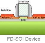
I recently spoke to Arvind Narayanan, Product Marketing Manager for Mentor’s place and route division about emerging technology. This of course led to FinFETS, FDSOI, performance, power, and cost-benefit. The battle between FDSOI and FinFETs, said Narayanan, is going to be something to watch.
Both FDSOI and FinFET technologies… Read More
Ground. It’s that little downward-pointing triangle that somehow works miracles on every schematic. It looks very simple until one has to tackle modern power distribution network (PDN) design on a board with high speed and high power draw components, and you soon discover ground is a complicated fairy tale with a lot of influences.… Read More
TSMC will host their annual technology symposium at several locations in the U.S. on April 9th in San Jose, April 16th in Austin, and April 23rd in Boston. TSMC will discuss the market outlook, design enablement, and technology for high-speed computing, mobile communications, connectivity and storage, CIS, embedded flash, … Read More
Amidst frequently changing requirements, time pressure and demand for high accuracy, it is imperative that EDA and design companies look at time consuming processes in the overall design flow and find alternatives without losing accuracy. High Frequency Analysis of IC designs is one such process which is traditionally based… Read More
This year’s Mentor Graphics user group meeting, User2User, will be held at the DoubleTree by Hilton in San Jose, California on April 25, 2013. The featured keynote presenters include…
- Dr. Walden C. Rhines, CEO and Chairman of Mentor Graphics, talking about “Organizing by Design”
- Victor Peng, Senior VP, Xilinx presenting on “The
…
Read More
Yesterday evening was the annual EDAC CEO forecast meeting. Actually it is not really a forecast meeting any more, more a sort of CEO response to some survey questions asked of EDAC members. Rich Valera of Needham moderated with Lip-Bu, Aart and Wally, along with Simon Segars representing the IP arm(!) of the business and Raul Camposano… Read More
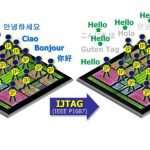
IJTAG for IP Test: a free seminarby Beth Martin on 03-14-2013 at 1:53 pmCategories: EDA, Siemens EDA
What: Better IP Test with IJTAG
When: 26 March, 2013, 10:30am-1:30pm
Where: Mentor Graphics, 46871 Bayside Parkway, Fremont, CA 94538
If you are involved in IC test*, you’ve probably heard about the IEEE P1687 standard, called IJTAG for ‘internal’ JTAG. IJTAG defines a standard for embedded IP that includes simple… Read More
Standard cell library characterization has been around for decades, Synopsys has been offering Liberty NCXand Cadence has Virtuoso Foundation IP Characterization. What’s new is that Mentor Graphics acquired the Z Circuit technology for library characterization and has integrated it with the Eldo Classic circuit … Read More
During DVCon I met with Steve Bailey to get an update on Mentor’s verification. They were also announcing some new capabilities. I also attended Wally Rhines keynote (primarily about verification of course, since this was DVCon; I blogged about that here) and the Mentor lunch (it was pretty much Mentor all day for me) on the… Read More
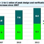
Wally Rhines gave the keynote at DVCon yesterday. He started out with a game of “name that graph” which was unfortunately a bit spoiled since when the names were revealed the first line was off the top of the screen. But he extrapolated several trends such as the decreasing number of fabs (the current trend is that there… Read More