
 I went to a couple more sessions at the Common Platform Technology Forum today, on 20nm double patterning and whatever will we do at 14nm. Basically, this is the end of planar transistors and the end of optical lithography. One session was by IBM scientists about process and one by Michael White of Mentor about double patterning. These two subjects turn out to be very related.
Double patterning will be required at 20nm because we are so far below the threshold for using 193nm light to print at the level of detail that single patterning requires. And everyone considers that betting on EUV to be ready for 14nm is very risky and so in the early days of 14nm we will use double patterning and then, if EUV works out, then we can switch to it and go back to single patterning.
The scary things about EUV is just how many things remain to be worked out. The source, which is plasma, is currently 1-2 orders of magnitude dimmer than is required. We don’t yet have good resist that responds to EUV. The masks, which are reflective, have defect issues since we can’t cover them with a pellicle like we can in a transmission mask. The masks are multi-layer films and even the blanks won’t be defect free. The scariest thing was a comment by Lars Liebmann of IBM: “I worked on X-ray lithography for years and EUV is not as far along as X-ray was when we finally discovered it wasn’t going to work.” We really don’t know if we can make EUV work and certainly not by the time it is needed for 14nm. A possible alternative, but equally sketchy in practice, is massively parallel e-beam.
The FinFET transistors will be much lower power. As the voltage drops, delay doesn’t go up nearly so much as with a planar transistor since they turn off so much more effectively and quickly. This means power supply voltage (squared in the dynamic power equation) can be lower for given performance.
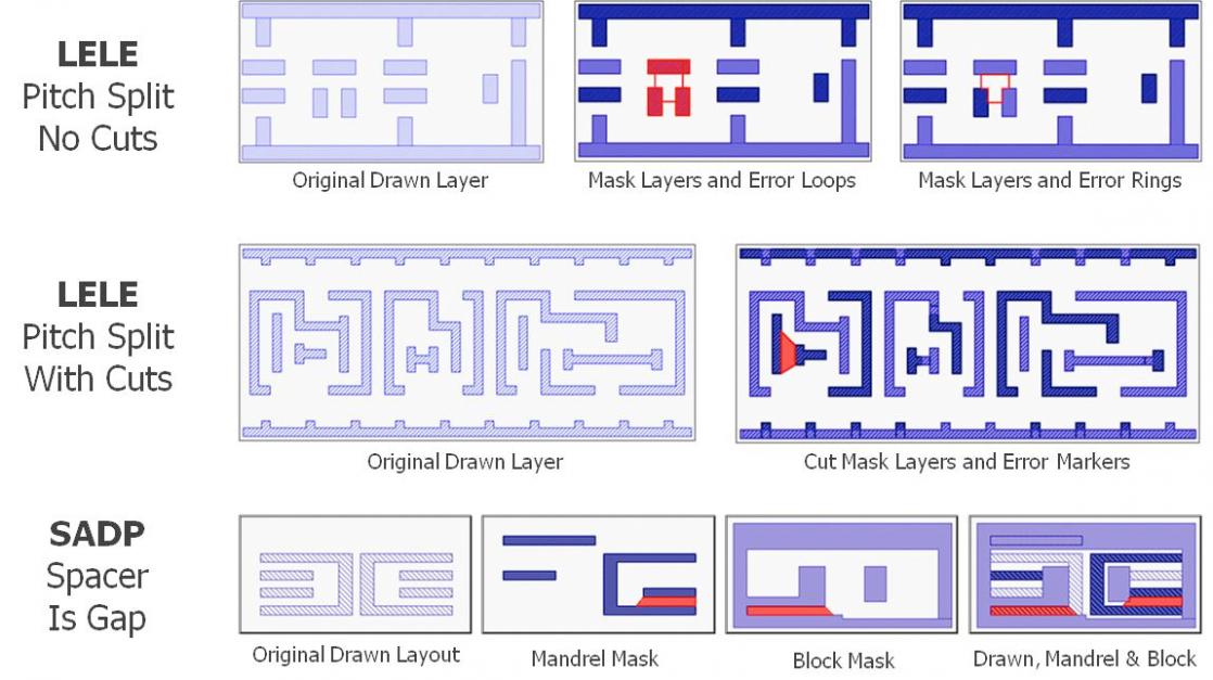
Double patterning means that half the polygons on the chip are on one mask and half on the other. It is not possible to simply expose the wafer to first one mask and then the other, there need to be etch steps in between and then a new photoresist exposed to the second mask. Since we really can’t live with just horizontal or just vertical metal on M1, this will need to be triple patterned with 3 masks.
Michael from Mentor started off in general terms pointing out that at every node the designer must address more and more manufacturability concerns. 20nm and 14nm are just more of the same. But double patterning does seem to be a major change, of course.
One challenge is how to reflect errors back to the user so that they can fix them. The problem occurs when 3 patterns are too close to each other but they can’t be put on separate masks. There are two solutions: redraw at least part of the layout, or split one of the polygons into two (cut and stitch) so that part goes on one mask and part on the other.
At 20nm we will also need smart cell-based fill rather than the old polygonal dummy fill, since the fill needs to be double pattern aware.
Mentor’s own place and route, Olympus, has a patterning aware placement that avoids putting cells too close and creating errors. I presume Cadence and Synopsys have, or will have, similar placement.
Mentor white papers on double patterning and other challenges are here.


Comments
0 Replies to “Double Patterning and Then The End of Lithography”
You must register or log in to view/post comments.