You are currently viewing SemiWiki as a guest which gives you limited access to the site. To view blog comments and experience other SemiWiki features you must be a registered member. Registration is fast, simple, and absolutely free so please,
join our community today!
WP_Term Object
(
    [term_id] => 157
    [name] => EDA
    [slug] => eda
    [term_group] => 0
    [term_taxonomy_id] => 157
    [taxonomy] => category
    [description] => Electronic Design Automation
    [parent] => 0
    [count] => 4534
    [filter] => raw
    [cat_ID] => 157
    [category_count] => 4534
    [category_description] => Electronic Design Automation
    [cat_name] => EDA
    [category_nicename] => eda
    [category_parent] => 0
    [is_post] =>
)
Synopsys is taking IP-SOC 2013 seriously, as the company will hold several presentations, starting with a Keynote: “Virtual Prototyping – A Reality Check”, by Johannes Stahl, Director, Product Marketing, System-Level Solutions, Synopsys, highlighting current industry practice around putting virtual prototyping to work… Read More
I am at ARM TechCon today. One interesting presentation was made jointly between Samsung, Cadence and ARM themselves about developing physical libraries (ARM), a tool flow (Cadence) and test chips (Samsung). It was titled Samsung ARM and Cadence collaborate on the silicon-proven world first 14-nm FinFET Cortex-A7 ARM CPU and… Read More
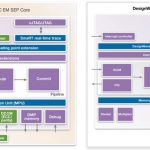
If you are familiar with Processor IP core, you certainly know DesignWare ARC EM4 core, 32-bit CPU that SoC designers can optimize for a wide range of uses, and differentiate by using patented configuration technology to tailor each ARC core instance to meet specific performance, power and area requirements. If you develop a product… Read More
You can often tell how important blogging and social media is to an EDA company by how much effort it takes to find their blog from the Home page. For the folks at Mentor Graphics I’d say that blogging is quite important, because it shows up as a top-level menu item. Notice also how important Twitter is, their latest tweets show… Read More
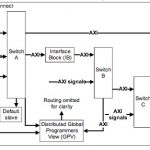
Semiconductor IP re-use enables modern SoC designs to be realized in a timely fashion, yet with hundreds of IP blocks in a chip the chances are higher that an error in any IP block could cause the entire system to fail. At advanced nodes like 28nm and smaller, the number of Process, Voltage and Temperature (PVT) corners is increasing… Read More
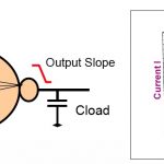
In the modern electronic world, it’s difficult to imagine any system working as a whole without MEMS (Micro-electromechanical Systems) such as pressure sensors, accelerometers, gyroscopes, microphones etc. working in sync with other ICs. Specifically in AMS (Analog Mixed-Signal) semiconductor designs, there can be significant… Read More
As semiconductors become more integrated into our lives reliability is becoming a critical issue. As IP consumes more of our die, IP reliability is becoming a critical issue. As we pack more transistors into a chip, reliability is becoming a critical issue. As we move from 28nm to 20nm to 16nm, reliability is becoming a critical … Read More
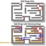
Diagnosing Double Patterning Violationsby Beth Martin on 10-28-2013 at 5:16 pmCategories: EDA, Siemens EDA
I’ll bet you’ve read a bunch of stuff about double patterning, and you’re probably hoping that the design tools will make all your double patterning issues just go away. Well, the truth is that the foundries and EDA vendors have worked really hard to make that true.
However, for some critical portions of your design, there … Read More
SoC designers are attracted to ARM as an IP provider because of their popular offerings and growing ecosystem of EDA partners like Carbon Design Systems. At the upcoming ARM Techcon on October 31 this week in Santa Clara you’ll have an opportunity to hear a joint presentation from ARM and Carbon Design Systems on: Getting … Read More
On October 10, I attended another Cadence Summit, this one titled the Cadence Mixed-Signal Technology Summit. Recently, I had written about the Cadence Silicon Verification Summit. The verification event was the first of its kind, and I thought it had terrific content. Being more of a digital guy myself, I was unaware that Cadence… Read More


The Silicon Shield Has Never Been Stronger!