The most successful EDA companies typically choose a domain where they have deep knowledge, then serve a few leading-edge customers that are willing to work with a start-up in exchange for early access to that new technology. The theory is that if you can satisfy the leading-edge customer then you can also satisfy the rest of the … Read More
Electronic Design Automation
Triple Patterning
As you can’t have failed to notice by now, 28nm is the last process node that does not require double patterning. At 20nm and below, at least some layers require double patterning. The tightest spacing is typically not the transistors but the local interconnect and, sometimes, metal 1.
In the litho world they call double patterning… Read More
Aldec the leader in DO254
I am convinced after studying out the matter, that Aldec is one of the leaders in DO254 certification. As you listen and read the news as I do about flight MA-370, you keep theorizing and wondering. This is a good time to introduce the reader to the seriousness of flight worthy electronics and the arduous process to achieve certification.… Read More
Social Media at Carbon Design Systems
Started in 2002 Carbon Design Systems has ESL (Electronic System Level) modeling and validation tools for complex SoC design. With their software you can:
- Perform system level model generation of existing and 3rd party IP directly from RTL for use in any virtual platform
- Do performance analysis & optimization of SoC architectures
Mentor U2U Is On April 10th
If you are a Mentor user, U2U, the Mentor User group is coming up on April 10th. This is an all day event at the DoubleTree. The event is free. Registration starts at 8am and the agenda itself starts at 9am. There is a reception from 5-6pm in the evening.
There are three keynotes. At 9am: Wally Rhines, CEO of Mentor. The Big Squeeze. For … Read More
A Fill Solution for 20nm at TSMC
By Jeff Wilson, Mentor Graphics
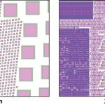
We’ve talked about the new requirements for Fill in IC design for advanced nodes in previous blogs on this site. This time I’d like describe the fill solution that Mentor and TSMC have jointly developed to meet the requirements of fill for TSMC’s 20nm (N20) manufacturing process.
The traditional… Read More
Xilinx & Apache Team up for FPGA Reliability at 20nm
In this age of SoCs with hundreds of IPs from different sources integrated together and working at high operating frequencies, FPGA designers are hard pressed keeping up the chip reliability from issues arising out of excessive static & dynamic IR drop, power & ground noise, electro migration and so on. While the IPs are… Read More
Cadence is all about Semiconductor IP!
Cadence continues on its quest to be a top semiconductor IP supplier which is a good thing since the semiconductor world now revolves around IP. Cadence CEO Lip-Bu Tan mentioned IP 14 times during his keynote and he was followed by the president of Imagination Technologies and the CEO of recently acquired Tensilica. I was not afforded… Read More
Getting 3D TV from 2D Content
3D TV has been all the rage over the past few years because of the added realism it offers the viewer, but there’s really not that much content that you can stream or play on a Blu-ray device. Wouldn’t it be cool if there was a box that could create 3D on the fly from a 2D stream or Blu-ray? This week I discovered that such a box… Read More
Jasper at DVCon and EJUG
The Jasper European User Group meeting (EJUG) is coming up in a couple of weeks. It will be held in the Munich Hilton (which I have stayed in many times, the S-bahn from the airport pretty much stops in the basement) on April 2nd.
The schedule for the day is:
9:00 AM – Registration and continental breakfast
9:30 AM – Jasper… Read More


Chemical Origins of Environmental Modifications to MOR Lithographic Chemistry