You are currently viewing SemiWiki as a guest which gives you limited access to the site. To view blog comments and experience other SemiWiki features you must be a registered member. Registration is fast, simple, and absolutely free so please,
join our community today!
WP_Term Object
(
    [term_id] => 157
    [name] => EDA
    [slug] => eda
    [term_group] => 0
    [term_taxonomy_id] => 157
    [taxonomy] => category
    [description] => Electronic Design Automation
    [parent] => 0
    [count] => 4439
    [filter] => raw
    [cat_ID] => 157
    [category_count] => 4439
    [category_description] => Electronic Design Automation
    [cat_name] => EDA
    [category_nicename] => eda
    [category_parent] => 0
    [is_post] =>
)
Tools, tools, tools. Designs are rapidly changing, JESD204b, Hybrid Memory cube and all other Gigabit serialization schemes are here to stay. RIP DDR. This means board level simulations with respect to firmware (FPGA) are going to be more challenging than ever. Why? you ask, especially if the board layout is simpler? True, but… Read More
So first the one thing that you do know. MunEDA are based in Munich which makes them German. I have to confess that until I got involved helping them a bit with some marketing stuff that that was about all I knew about them too.
So now five things that you might not know:
1. MunEDA have a much wider customer list that you know and would even… Read More
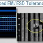
Although semiconductor manufacturing has taken off with FinFET based process technology which provides lucrative payoffs on performance improvement, power reduction and area saving in devices for high density and high performance SoC demand of modern era, apprehensions remain about its reliability due to reduced noise … Read More
I first met Dundar Dumlugolat Barcelona Design back in 2004, so it was a pleasure to meet with him again at DAClast week and learn more about what his company Magwel has to offer IC designers of power management chips.… Read More
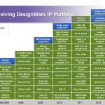
Synopsys has been extremely active, during the last 10 years, not only launching new IP products every year, but also running an ambitious acquisition strategy, with no less than 8 acquisitions. Cascade acquisition bring PCI Express (controller only), when Accelerant bring SerDes (the earth of any PHY IP). The MIPS/Chipidea… Read More
It was a bad sign when an EDA company solicited John Cooley’s help in their legal challenge: See Did Atoptech Just Astroturf Synopsys? Gabe Moretti also did an article: John Cooley Barrister Chastises Synopsys | Gabe on EDA. An even worse sign is when your legal team gets disqualified, especially when that legal team is the top EDA… Read More
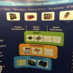
MEMS Update from DACby Daniel Payne on 06-11-2014 at 11:32 amCategories: Coventor, EDA
DAC has an interesting mix of vendors each year, and some of them are outside of the expected digital, analog or IP space. Last Tuesday at DAC I visited a company called Coventor that has three product lines:
…
Read More
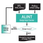
Even though I live just 7 miles away from the Mentor Graphics corporate office in Oregon, I visited their DAC suite in San Francisco last week to get an update on Calibrefrom Michael White. The Calibre tools are used during IC verification and sign-off by performing DRC (Design Rule Checking) and LVS (Layout Versus Schematic).… Read More
In recent days I’ve seen several long discussions about Texas Instrumentslosing its grip in semiconductor industry when it came out of a business it was strong in, i.e. wireless business. It seems the semiconductor community has not digested the fact that TI, very rightly, came out of the OMAP business at the right time. The smartphone… Read More
I was a the embedded vision conference last week. Jeff Beir, the founder of the embedded vision alliance gave an introduction to the field. The conference was much bigger than previous years and almost everyone is designing some sort of vision product. Half of your brain is used for vision so it goes without saying that vision requires… Read More


Chemical Origins of Environmental Modifications to MOR Lithographic Chemistry