You are currently viewing SemiWiki as a guest which gives you limited access to the site. To view blog comments and experience other SemiWiki features you must be a registered member. Registration is fast, simple, and absolutely free so please,
join our community today!
WP_Term Object
(
    [term_id] => 157
    [name] => EDA
    [slug] => eda
    [term_group] => 0
    [term_taxonomy_id] => 157
    [taxonomy] => category
    [description] => Electronic Design Automation
    [parent] => 0
    [count] => 4440
    [filter] => raw
    [cat_ID] => 157
    [category_count] => 4440
    [category_description] => Electronic Design Automation
    [cat_name] => EDA
    [category_nicename] => eda
    [category_parent] => 0
    [is_post] =>
)
When I hear the phrase Static Timing Analysis (STA) the first EDA tool that comes to mind is PrimeTimefrom Synopsys, and this type of tool is essential to reaching timing closure for digital designs by identifying paths that are limiting chip performance. Sunil Walia, PrimeTime ADV marketing lead spoke with me by phone on Thursday… Read More
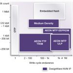
As of today NVM IP has been mostly used in SoC or IC to support very specific needs like analog trimming and calibration or encryption key integration for Digital Right Management (DRM) purpose. In other words small size (less than 1K-bit) few times programmable (FTP) NVM IP was enough to support these needs, thus most of the NVM IP… Read More
DNA sequencing — which provides vital information on genetics study, forensics, diagnostics and therapies — has been an exclusive territory of high-end research labs with millions of dollars to spend because of the expensive chemical and optical equipment needed for research. That is changing, thanks to complex… Read More
When chip designers moved from a gate-level design methodology to coding with RTL there was a learning curve involved, and the same thing happens when you move from RTL to High Level Synthesis (HLS) using C++ or SystemC coding. One great shortcut to this learning curve is the use of pre-defined library functions. I just heard about… Read More
It was back in July of 2012 that the acquisition of Sigrity by Cadence was announced. Although Cadence is a dominant player in both IC and board layout tools, they did not have an electromagnetic (EM) signal integrity solution in their portfolio. This acquisition marks a turning point for the EM/SI sector – tight integration… Read More
ANSYS makes a big deal of being a multi-physics company. Still it has taken them a while to fully integrate Apache. Nevertheless it seems like there is a compelling argument for combining technologies to solve SOC design problems. Frankly most chip designers would be hard pressed to think of a reason for using computational fluid… Read More
Silvaco TCAD Webinarby admin on 01-26-2015 at 4:50 pmCategories: EDA
TCAD is a somewhat specialized area since not that many people design semiconductor processes compared to the number who design chips. Bit without TCAD there would be no chips. One area where the two domains intersect is that of SEE, where neutrons (mainly) can cause a flop or a memory bit to change. Since we live on a radioactive planet… Read More
Although CMOS technology in semiconductors was patented in 1960s, commercial ICs and electronic systems based on CMOS ICs started picking up in 1970s, and the real growth with personal computer (PC) market took place in 1980s. Then Intelmicroprocessors started dominating the semiconductor market with increasing processing… Read More
Measuring Metastabilityby Jerry Cox on 01-24-2015 at 7:00 amCategories: EDA
Measuring metastability is just 50 years old this year. In 1965 my colleague Tom Chaney took a sampling ‘scope picture of an ECL flip-flop going metastable. S. Lubkin had made mention of the phenomenon over a decade before that, but at that time most engineers were unaware of the phenomenon or did not believe it actually existed. … Read More
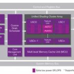
We have been hearing for some time about the Synopsys HAPS-70 and how they have co-created the hardware and software architecture for FPGA-based prototyping with their customers. Now, we see details published by Synopsys on how they collaborated with Imagination on the design of the PowerVR Series6XT GPU.
The first thing to come… Read More


Silicon Insurance: Why eFPGA is Cheaper Than a Respin — and Why It Matters in the Intel 18A Era