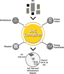
I read the semiconductor press, LinkedIn and social media (Twitter, Facebook) every morning along with an RSS feed that I setup, staying current on everything related to using EDA tools to make the task of SoC design a bit easier for design teams. A recent press release announced a tool called SoC Compiler, so my curiosity was piqued… Read More
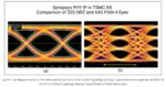
PCI-SIG has held to doubling PCIe’s data rate with each revision of the specification. The consortium of 800 companies, with its board consisting of Agilent, AMD, Dell, HP, Intel, Synopsys, NVIDIA, and Qualcomm, is continuing this trend with the PCIe 6.0 specification which calls for a transfer rate of 64 GT/s. PCI-SIG released… Read More
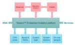
SoC integration offers huge benefits through reduced chip count in finished systems, higher performance, improved reliability, etc. A single die can contain billions of transistors, with multiple processors and countless subsystems all working together. The result of this has been rapid growth of semiconductor content … Read More
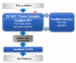
In business we all have heard the maxim, “Time is Money.” I learned this lesson early on in my semiconductor career when doing DRAM design, discovering that the packaging costs and time on the tester were actually higher than the fabrication costs. System companies like IBM were early adopters of Design For Test (DFT)… Read More
Verification Challenge
As chip design complexity continues to grow astronomically with hardware accelerators running riot with the traditional hardware comprising CPUs, GPUs, networking and video and vision hardware, concurrency, control and coherency will dominate the landscape of verification complexity for safe … Read More
Dan is joined by Frank Schirrmeister, senior group director of solutions marketing at Cadence Design Systems, Frank has extensive experience in complex system design from his work at companies such as Cadence, Synopsys, Imperas and ChipVision. He has also advised Vayavya Labs and CriticalBlue.
Dan and Frank discuss the many… Read More
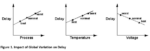
We have come a long way from the days of limited and manageable characterization databases with fewer views and smaller library sizes. The technologies we are headed towards pushing characterization to its limits with special modeling for variation, aging and reliability all on a single process, voltage and temperature (PVT).… Read More
Siemens EDA’s Veloce emulation products are long-established and worthy contenders in any emulation smack-down. But there was always a hole in the complete acceleration story. Where was the FPGA prototyper? Current practice requires emulation for fast simulation with hardware debug, plus prototyping for faster simulation… Read More


Silicon Insurance: Why eFPGA is Cheaper Than a Respin — and Why It Matters in the Intel 18A Era