You are currently viewing SemiWiki as a guest which gives you limited access to the site. To view blog comments and experience other SemiWiki features you must be a registered member. Registration is fast, simple, and absolutely free so please,
join our community today!
WP_Term Object
(
    [term_id] => 157
    [name] => EDA
    [slug] => eda
    [term_group] => 0
    [term_taxonomy_id] => 157
    [taxonomy] => category
    [description] => Electronic Design Automation
    [parent] => 0
    [count] => 4439
    [filter] => raw
    [cat_ID] => 157
    [category_count] => 4439
    [category_description] => Electronic Design Automation
    [cat_name] => EDA
    [category_nicename] => eda
    [category_parent] => 0
    [is_post] =>
)
Standards help our EDA and IP industry grow more quickly and with less CAD integration efforts, and IP-XACT is another one of those Accellera standards (1685-2009) that is coming of age, and enabling IP reuse for SoC design teams. Here at SemiWik, we’ve been writing about Defacto Technologies and their prominent use of IP-XACT… Read More
Introduction
Frequent SemiWiki readers are aware of the growing significance of heterogeneous multi-die packaging technologies, offering a unique opportunity to optimize system-level architectures and implementations. The system performance, power dissipation, and area/volume (PPA/V) characteristics of a multi-die… Read More
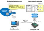
Using FPGAs to prototype and debug SoCs as part of the SoC design verification hierarchy was pioneered by Quickturn Design Systems in the late 1980’s, and I have observed a wide variety of FPGA prototyping projects over the years. In retrospect, three factors have determined the success of the FPGA prototyping project;
- A good
…
Read More
The truth is that we are just at the beginning of the Artificial Intelligent (AI) revolution. The capabilities of AI are just now starting to show hints of what the future holds. For instance, cars are using large complex neural network models to not only understand their environment, but to also steer and control themselves. For… Read More
Automatic Place and Route (APR) tools have been around since the 1980s for IC design teams to use, and before that routing was done manually by very patient layout designers. Initially the big IDMs had their own internal CAD groups coding APR tools in house, but eventually the commercial EDA market picked up this automation area,… Read More
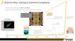
The electronic design community is well aware that it faces a daunting challenge to analyze and sign off the next generation of huge multi-die 3D-IC systems. Most of today’s EDA tools require extraordinary resources in specialized computers with terabytes of RAM and hundreds of processors. Customers don’t want to keep buying… Read More
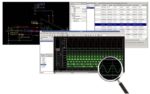
We all know that project planning and tracking are critical for any complex undertaking, especially a complex SoC design project. We also know that IP management is critical for these same kinds of projects – there is lots of IP from many sources being integrated in any SoC these days. If you don’t keep track of what you’re using and… Read More
You probably know the value proposition for using AI and ML (machine learning) in simulation regressions. There are lots of knobs you can tweak on a simulator, all there to help you squeeze more seconds, or minutes out of a run. If you know how to use those options. But often it’s easier to talk to your friendly AE, get a reasonable default… Read More
Ansys HFSS™ has long enjoyed industry respect as a highly accurate electromagnetic simulator suitable for general purpose applications. Ansys has worked over the years to maintain its gold reference accuracy, and also to dramatically improve its performance and ease of use. A very interesting review of the key technology breakthroughs… Read More
Automotive electronics bring strong demand for power management chips, but its strict reliability requirements also pose new challenges for chip designers. The chip needs to be able to work in various harsh environments such as high temperature, low temperature, aging, abnormal power supply, etc. Although the traditional… Read More


Silicon Insurance: Why eFPGA is Cheaper Than a Respin — and Why It Matters in the Intel 18A Era