You are currently viewing SemiWiki as a guest which gives you limited access to the site. To view blog comments and experience other SemiWiki features you must be a registered member. Registration is fast, simple, and absolutely free so please,
join our community today!
WP_Term Object
(
    [term_id] => 157
    [name] => EDA
    [slug] => eda
    [term_group] => 0
    [term_taxonomy_id] => 157
    [taxonomy] => category
    [description] => Electronic Design Automation
    [parent] => 0
    [count] => 4439
    [filter] => raw
    [cat_ID] => 157
    [category_count] => 4439
    [category_description] => Electronic Design Automation
    [cat_name] => EDA
    [category_nicename] => eda
    [category_parent] => 0
    [is_post] =>
)
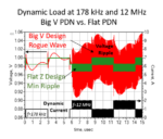
Advanced board designs are fertile ground for misbehavior in time and frequency domains. Relying on intuition, then waiting until near-final product for power integrity (PI) or EMI testing almost guarantees board respins are coming. Lumped-parameter simulations of on-board power delivery networks (PDNs) struggle with … Read More
I’ve been following Neil Johnson on Twitter and LinkedIn for several years now, as he has written and shared so much about the IC design and verification process, both as a consultant and working at EDA vendors. His recent white paper for Siemens EDA caught my eye, so I took the time to read through the 10 page document to learn… Read More
The great thing about architectural solutions to increasing throughput is that they offer big improvements. Multiple CPUs on a chip with (partially) shared cache hierarchies are now commonplace in server processors for this reason. But that big gain comes with significant added complexity in verifying correct behavior. In… Read More
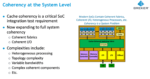
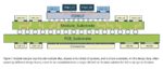
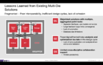
Multi-chip modules are now more important than ever, even though the basic concept has been around for decades. With The effects of Moore’s Law and other factors such as yield, power, and process choices, reasons for dividing what once would have been a single SOC into multiple die and integrating them in a single module have become… Read More
Multi-die design is not a new concept. It has been around for a long time and has evolved from 2D level integration on to 2.5D and then to full 3D level implementations. Multiple driving forces have led to this progression. Whether the forces are driven by market needs, product needs, manufacturing technology availability or EDA… Read More
Automatic adaptive meshing in Ansys HFSS is a critical component of its finite element method (FEM) simulation process. Guided by Maxwell’s Equations, it efficiently refines a mesh to deliver a reliable solution, guaranteed. Engineers around the world count on this technology when designing cutting-edge electronic products.… Read More
The old phrase that the cure is worse than the disease is apropos when discussing MBIST for large SOCs where running many MBIST tests in parallel can exceed power distribution network (PDN) capabilities. Memory Built-In Self-Test (MBIST) usually runs automatically during power on events. Due to the desire to speed up test and … Read More
As the oldest and largest EDA conference, the Design Automation Conference (DAC) brings the best minds together to present, discuss, showcase and debate the latest and greatest advances in EDA. It accomplishes this in the form of technical papers, talks, company booths, product pavilions and panel discussions.
A key aspect … Read More
There has been a lot of attention in the news recently about AT&T and Verizon rolling out their first implementations of sub-6GHz 5G radio access networks (RAN). Notably, the FAA and airline industries have voiced serious concerns about potential safety issues for aircraft autopilot and landing systems. As a result of these… Read More
As we established last year, we will use the January issue of this blog to look back at the papers we reviewed last year. We lost Jim Hogan and the benefit of his insight early last year, but we gained a new and also well-known expert in Raúl Camposano (another friend of Jim). Paul (GM, Verification at Cadence), Raúl (Silicon Catalyst,… Read More


Silicon Insurance: Why eFPGA is Cheaper Than a Respin — and Why It Matters in the Intel 18A Era