
If I was asked about must-have needs for 5G, I’d probably talk about massive MIMO and a lot of exotic parallel DSP processing, also perhaps need for new intelligent approaches to link adaptation and intelligent network slicing in the infrastructure. But there’s something that comes before that all that digital cleverness, in the RF front-end, which has also become pretty exotic. This is the filter(s). These are the devices that pluck out an RF channel of interest from the surrounding radio cacophony and ignore everything else.
Filters at this level look nothing like conventional circuits, either analog or digital. They operate on a piezoelectric substrate; an electric transducer (driven by the input radio signal) at one end stimulates mechanical action and thus an acoustic wave. This travels to the other end where that wave triggers a second transducer, converting the acoustic signal back into an electrical signal.
Might seem like a lot of work to accomplish not very much, however the magic is in managing those acoustic waves. Like a tiny musical instrument, the filter (plus a cavity underneath) has a narrow band of resonant frequencies; everything outside that frequency range is damped into non-existence. And as for musical instruments, the resonance range depends on the mechanical design of the device – dimensions, thicknesses, material and the cavity.
2G, 3G and 4G front-ends have used surface acoustic wave (SAW) filters in which the wave travels along the surface of the device. These are apparently very cost effective but are limited to frequencies below ~2GHz, where filter selectivity begins to decline. This is fine for 3G, on the edge for 4G and not good enough for 5G. That’s pushed a switch to bulk acoustic wave (BAW) filters which can support higher frequencies, at somewhat higher costs.
One reason for that cost may be the complexity of designing such filters. You see, these are really MEMS devices since they’re electromechanical; even though you don’t see anything moving, the acoustic waves are mechanical distortions in the piezoelectric (PE) structure. A typical filter is a thin film of PE between two electrodes, sitting on top of the cavity. I’ve talked before about the challenges in designing MEMS – no pre-characterized cells or nicely defined PDKs from which you can reliably model.
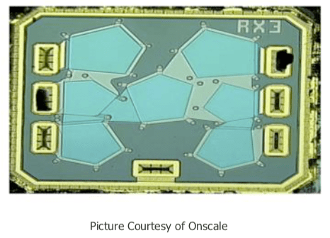
There’s a second problem. Acoustic waves go where they want to go. While a square or rectangular structure might seem like the logical way to build these things, waves can reflect off ends, and can also run in the surface. Either effect may contaminate the ideal bulk behavior. So structures are built with interesting shapes like irregular pentagons (see above), to damp out undesired behaviors. Also it’s common to build networks of resonators, each of which can have a different geometry.
Now you see the problem – electromechanical 3D modeling (because you’re modeling bulk and surface acoustic waves), through strange geometries with little reference data to guide your models. I was told that some of the leading companies producing these filters are still using a design-fab-analyze-correct loop to get to optimized designs. There has been no better way. But it’s still been worth it because the volumes for these devices are huge – one (or more?) in every 5G edge device, including cellphones.
But now there is a better way, and that’s important because that development loop also affects time to market in what are commonly winner-take-all markets (at least per model release). That is to virtually prototype these devices, starting from a custom-characterized PDK.
Which is what the Mentor/Tanner-SoftMEMS-OnScale solution does well. You design the device, layer by layer in Ledit (which incidentally does well at handling strange shapes like irregular pentagons), convert that to a 3D model by adding materials definitions, piezo properties through matrices, thicknesses, process data, mechanical properties and boundary conditions, then model the whole thing, or just a part of it, in the cloud using the scalable FEA analytics from OnScale. Mary Ann (SoftMEMS) told me they can even model a full wafer, looking for behaviors and yield hits around the edges.
Better virtual modeling and better analytics, all the way up to wafer-scale analysis. That should help reduce time-to-market. You can learn more about this flow HERE.
Share this post via:


Comments
There are no comments yet.
You must register or log in to view/post comments.