You are currently viewing SemiWiki as a guest which gives you limited access to the site. To view blog comments and experience other SemiWiki features you must be a registered member. Registration is fast, simple, and absolutely free so please,
join our community today!
WP_Term Object
(
    [term_id] => 19172
    [name] => Chiplet
    [slug] => chiplet
    [term_group] => 0
    [term_taxonomy_id] => 19172
    [taxonomy] => category
    [description] =>
    [parent] => 0
    [count] => 195
    [filter] => raw
    [cat_ID] => 19172
    [category_count] => 195
    [category_description] =>
    [cat_name] => Chiplet
    [category_nicename] => chiplet
    [category_parent] => 0
    [is_post] =>
)
Anna has more than 25 years of expertise in managing complex R&D organizations and programs, giving birth to a number of innovative EDA technologies. She has pioneered the study and development of several generations of IC and package co-design environments and has held senior positions at leading semiconductor and EDA … Read More
Semiconductor industry is going through an unprecedented technological revolution with AI/ML, GPU, RISC-V, chiplets, automotive and 5G driving the hardware design innovation. The race to deliver high performance, optimizing power and area (PPA), while ensuring safety and security is truly on. It has never been a more exciting… Read More
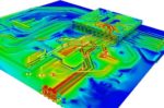
As one of the world’s leading chip foundries, Samsung occupies a vital position in the semiconductor value chain. The annual Samsung Advanced Foundry Ecosystem (SAFE™) Forum is a must-go event for semiconductor and electronic design automation (EDA) professionals. Ajei Gopal, President and CEO of Ansys, has the honor of delivering… Read More
Chiplets continue to be a hot topic on SemiWiki, conferences, white papers, webinars and one of the most active chiplet enabling vendors we work with is Synopsys. Synopsys is the #1 EDA and #1 IP company so that makes complete sense.
As you may have read, I moderated a panel on Chiplets at the last SNUG which we continue to write about.
…
Read More
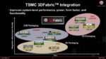
Last week TSMC announced the opening of an advanced backend fab for the expansion of the TSMC 3DFabric System Integration Technology. It’s a significant announcement as the chip packaging arms race with Intel and Samsung is heating up.
Fab 6 is TSMC’s first all-in-one advanced packaging and testing fab which is part of the… Read More
In the 3D-IC (Three-dimensional integrated circuit) chip design method, chiplets or wafers are stacked vertically on top of each other and are connected using Through Silicon Vias (TSVs) or hybrid bonding.
The 2.5D-IC design method places multiple chiplets alongside each other on a silicon interposer. Microbumps and interconnect… Read More
Join this webinar and see UCIe in action! This webinar presents the SystemVerilog models of a Universal Chiplet Interconnect Express (UCIe) interface, including both the analog circuits in the electrical layer and digital FSMs in the logical layer. The whole physical layer (PHY) model can be efficiently simulated in SystemVerilog,… Read More
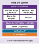
For decades now I’ve watched the incredible growth of SoCs in terms of die size, transistor count, frequency and complexity. Instead of placing all of the system complexity into a single, monolithic chip, there are now compelling reasons to use a multi-chip approach, like when the maximum die size limit is reached, or it’s… Read More
At the recent Synopsys Users Group Meeting (SNUG) I had the honor of leading a panel of experts on the topic of chiplets. One of those panelists was John Lee, Head of Electronics, Semiconductors and Optics at Ansys.
How is the signoff flow evolving and what is being done to help mitigate the growing signoff complexity challenge?
With… Read More
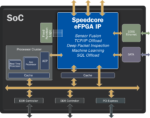
With our continuing chiplet coverage I found this of great interest. I have always felt that eFPGAs and chiplets are a natural fit for the next generation of chip design and this is an excellent example. As we design with chiplets one of the challenges is verification/validation in regards to performance and interoperability. … Read More


Silicon Insurance: Why eFPGA is Cheaper Than a Respin — and Why It Matters in the Intel 18A Era