Semiwiki readers are no doubt very familiar with the increasing impact of the automotive market on the semiconductor industry. The magnitude and complexity of the electronic systems that will be integrated into upcoming vehicle designs reflects the driver automation, safety, and entertainment features that are in growing demand. The figure below illustrates the anticipated “value” of the electronics that will be present in future years.

Foundries are focusing process development and design enablement resources on the unique requirements associated with the harsh environments associated with the different automotive quality product “grades”, as established by the Automotive Electronics Council AEC-Q100 standard:
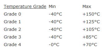
The AEC_Q100 standard document is located at this link.
IP providers are also focusing on ensuring their designs are qualified for this quality standard, as well.
In addition to this emphasis by the foundries and the IP providers, there are also (perhaps less well-known) actions being undertaken by EDA companies to address the related tool requirements for the automotive market.
A colleague recently recommended that I should review some of the (automotive-focused) initiatives at Mentor, a Siemens company. Among the product development features that have recently been pursued, there were two that I wanted to highlight, as they are indeed both innovative and crucial to achieve the required automotive IC product quality goals.
Analog IP Test
Speaking of product quality, ON Semiconductor recently shared the following insightful data — see the figure below.
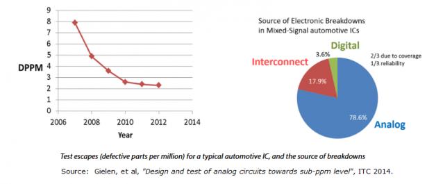
The test escape defects in PPM for automotive IC’s is plateauing, suggesting that further improvements will require new methodologies. And, the source of the defects is overwhelmingly in the analog IP blocks. Clearly, an emphasis on automating analog fault coverage is needed.
A couple of years ago, Mentor introduced Cell-Aware Testfeatures into their Tessent Automated Test Pattern Generation (ATPG) product family. The key to this enhancement was the focus on identifying the significant R and C elements in the parasitic extracted netlist for a cell, and introducing resistive changes associated with manufacturing defects to the characterization netlist — e.g., high resistance value substitution for R’s to reflect an open, and low resistance values across C’s to reflect a short. Tessent was also enhanced to accept a User Defined Fault Model (UDFM), where the design team could introduce specific internal faults within cells submitted to ATPG algorithms.
Mentor has built upon this expertise to address the analog test escape issue highlighted above, with the introduction of Tessent DefectSim. I found the following features in DefectSim to be extremely novel:
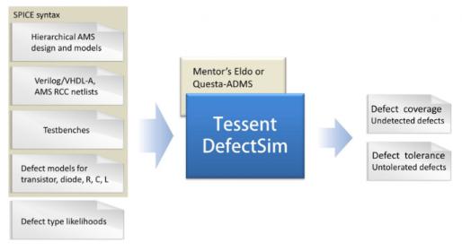
(1) Likelihood Weighted Random Sampling (LWRS) to select analog faults to inject into the model
Although the potential number of analog “faults” in a complex IP block is large, manufacturing opens and shorts remain the prevalent defects. (The space of device parametric variations across a design is huge — the assumption is that the fabrication process control monitors will be used to keep the devices within their specified statistical tolerances, and the design will have been simulated to meet specifications across those device variations.)
Mentor has leveraged their insight into modeling these defects with resistance changes to the extracted analog IP netlist. However, unlike digital ATPG algorithms that exercise stuck-at-0/stuck-at-1 fault injection throughout, analog IP fault detection relies upon circuit simulation to evaluate whether the block continues to meet its specifications. And, since analog IP simulation testbenches can be extensive (especially when considering the number of corners), there is a need to identify an appropriate sample of defects to inject for simulation.
In DefectSim, parasitic elements are first grouped based upon common characteristics — e.g., wire length, area spanned, number of circuit nodes connected to the element. In addition, there are transistor faults associated with shorts and opens between gate, drain, and source nodes. From each group, a sample of defects are selected for simulation using a weighted likelihood — e.g., coupling C’s from adjacent wires with a long parallel run length are more likely candidates for a short defect. As a result, there is fault coverage within each group, sampling the most likely defects within that group.
After simulating with the sampled defects, a statistical coverage measurement (and confidence level) is provided by DefectSim.
(2) DefectSim simulation efficiency features
Since analog fault detection is simulation-based, throughput is a key concern. In addition to statistical fault sampling, DefectSim offers a number of capabilities:
- parallel simulation of models with different injected fault
- intelligent hierarchical model build, where the designer can select higher-level models for blocks in the analog IP hierarchy that do not contain the injected fault (e.g., schematic, Verilog-A, Verilog-AMS)
- DC, AC, or transient simulations can be selected, as appropriate for the testbench and injected fault
- stop-on-detection (stop simulation when a specification measurement failure is observed, or a digital logic value difference is recorded)
- intelligent “corner management” (simulate defects at the typical corner first, then only pursue corner simulations for undetected faults)
(3) Additional model and simulation diagnostic features
- an open is modeled as a high resistance, plus a leakage resistor to a rail (prevents floating simulation nodes)
- additional simulation measures are added with the defect, to guide testbench selection (if the voltage across the defect element differs only slightly from the defect-free model simulation, the controllability/observability of the defect by the test is weak)
- schematic netlists can be used without waiting for extracted layout parasitics; designers can analyze transistor faults and/or leverage the “user defined fault model” strategy to provide circuit variations (e.g., an open connection among a capacitor array would decrease the total capacitance by a significant margin)
The capability to add automation (and statistical coverage measurement) to analog IP will be crucial to reducing the DPPM of production parts, a critical requirements for the growth of the automotive market… or, for that matter, to any SoC integrating complex analog IP blocks.
Mentor SAFE Program
I was also encouraged to learn more about the dedicated emphasis within Mentor on tool qualification, as per the ISO 26262 standard for automotive systems. The standard covers a much broader scope than just the safety-critical nature of the Tier 1 products that are supplied to automobile manufacturers — it extends to the EDA software tools that are used by the Tier 1 providers are part of their design flows, as well (ISO 26262 Part 8, Section 11 — Supporting Processes).
Briefly, the Mentor SAFE program adopts a formal method for documenting how Mentor tool releases are tested and qualified. Workflows and customer use cases are identified that are cross-referenced to qualification testing within Mentor.
Mentor tools are classified in terms of the confidence level for two facets:
[LIST=1]
These confidence levels are supported by the qualification testing and documentation.
In short, SoC design program managers will want to review the Mentor SAFE qualification documentation as to the scope of the workflow tool chain, the use cases, and the tool environment used. The Mentor SAFE initiative provides the level of design flow confidence that are required by demanding safety standards.
There are several Mentor whitepapers and sites worth investigating further, regardless of your type of design:
Automotive Products initiative
–chipguy
Share this post via:


Comments
2 Replies to “Automotive IC Design Requires a Unique EDA Tool Emphasis”
You must register or log in to view/post comments.