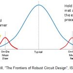
The impact of process variation at advanced nodes is increasing — no surprise there. In recent years, the principal design emphasis to better reflect this variation has been the adoption of two new methodologies: (1) advanced on-chip variation (AOCV, as well as POCV/LVF) for digital static timing analysis, and (2) advanced… Read More
Author: Tom Dillinger
Custom Layout Productivity Gets a Boost
In the 1970’s, when Moore’s Law was still in its infancy, Bill Lattin from Intel published a landmark paper [1]. In it he identified the need for new design tools and methods to improve layout productivity, which he defined as the drawn and verified number of transistors per day per layout designer. He said existing … Read More
Analog Design Verification — Traceability is Required
Digital verification engineers have developed robust, thorough metrics for evaluating design coverage. Numerous tools are available to evaluate testbenches against RTL model descriptions — e.g., confirming that simulation regressions exhaustively exercise signal toggles, RTL statement lines, individual statement… Read More
PCB Design Requires Both Speed and Accuracy of SI/PI Analysis
The prevailing industry trends are clear: (1) PCB and die package designs are becoming more complex, across both mobile and high-performance applications; (2) communication interface performance between chips (and their related protocols) is increasingly demanding to verify; (3) signal integrity and power integrity issues… Read More
The Latest in Static Timing Analysis with Variation Modeling
In many ways, static timing analysis (STA) is more of an art than a science. Methodologists are faced with addressing complex phenomena that impact circuit delay — e.g., signal crosstalk, dynamic I*R supply voltage drop, temperature inversion, device aging effects, and especially (correlated and uncorrelated) process… Read More
Bridging Design Environments for Advanced Multi-Die Package Verification
This year is shaping up to be an inflection point, when multi-die packaging technology will experience tremendous market growth. Advanced 2.5D/3D package offerings have been available for several years, utilizing a variety of technologies to serve as the package substrate, interposer material for embedding die micro-bump… Read More
Improvements in SRAM Yield Variation Analysis
The design of an SRAM array requires focus on the key characteristics of readability, writeability, and read stability. As technology scaling has enabled the integration of large (cache) arrays on die, the sheer number of bitcells has necessitated a verification methodology that focuses on “statistical high-sigma” variation… Read More
Key Takeaways from the TSMC Technology Symposium Part 2
In Part 1, we reviewed four of the highlights of the recent TSMC Technology Symposium in San Jose. This article details the “Final Four” key takeaways from the TSMC presentations, and includes a few comments about the advanced technology research that TSMC is conducting.… Read More
Analog Mixed-Signal Layout in a FinFET World
The intricacies of analog IP circuit design have always required special consideration during physical layout. The need for optimum device and/or cell matching on critical circuit topologies necessitates unique layout styles. The complex lithographic design rules of current FinFET process nodes impose additional restrictions… Read More
Key Takeaways from the TSMC Technology Symposium Part 1
TSMC recently held their annual Technology Symposium in San Jose, a full-day event with a detailed review of their semiconductor process and packaging technology roadmap, and (risk and high-volume manufacturing) production schedules.… Read More


Agentic AI Demands More Than GPUs