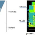
The SoC designs of today are much more complex than ever in terms of number of clocks, IPs, levels of hierarchies, several modes of operations, different types of validations and checks for growing number of constraints at various stages in the design flow. As a semiconductor design evolves through several stages from RTL to layout,… Read More
Author: Pawan Fangaria
SEMulator3D 2014 – New Enhancements for Virtual Fabrication in the 3D IC Era
A Virtual Platform for any kind of design or manufacturing in any discipline of science or engineering (electrical, mechanical, aeronautics etc.) must be able to provide an accurate representation of an actual design/product in a fraction of time and cost it takes to build working prototypes. In the case of semiconductors at … Read More
Imagine what all the DLP technology can do for you
Light has become integral part of most of the electronic devices we use today in any sphere of influence; personal, entertainment, consumer, automotive, medical, security, and industrial and so on. It’s obvious; along with IoT (Internet-of-Things) devices, the devices to illuminate and display things will play a major role… Read More
Evaluate MEMS Devices out-of-fab Before Fabrication
MEMS design and fabrication is highly complex in the sense that the fabrication process heavily depends on the design, unlike IC fabrication which has a standard set of processes. A slight change in MEMS design can alter its fabrication steps to a large extent. For example, setting device parameters such as capacitance or linear… Read More
Xilinx & Apache Team up for FPGA Reliability at 20nm
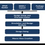
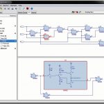
In this age of SoCs with hundreds of IPs from different sources integrated together and working at high operating frequencies, FPGA designers are hard pressed keeping up the chip reliability from issues arising out of excessive static & dynamic IR drop, power & ground noise, electro migration and so on. While the IPs are… Read More
Mark your Date for Semiconductor Design Vision
A very popular acronym is ‘WYSIWYG’ – What You See Is What You Get! This is very true and is important to visualize things to make it better in various aspects such as aesthetics, compactness, organization, structure, understandable for correction and so on; the most important, in case of semiconductor design, is being able to identify… Read More
A Tool Conceived With Designers’ Input and Developed from Scratch
If we look at the past, most of the EDA tools in the semiconductor design space have originated from a designers’ need to do things faster. Regardless of whether it is design exploration, manual design, simulation, verification, optimization (Power Performance Area – PPA) and many other steps in the overall design flow.… Read More
Effective Verification Coverage through UVM & MDV
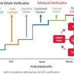
In the current semiconductor design landscape, the design size and complexity of SoCs has grown to large extent with stable tools and technologies that can take care of integrating several IPs together. With that mammoth growth in designs, verification flows are evolving continuously to tackle the verification challenges … Read More
Semiconductor Strategy – From Productivity to Profitability
The semiconductor industry seems to be the most challenged in terms of cost of error; a delay of 3 months in product development cycle can reduce revenue by about 27% and that of 6 months can reduce it by almost half; competition is rife, pushing the products to next generation (with more functionality, low power, high performance,… Read More
How to meet 3Ps in 3D-ICs with sub-20nm Dies?
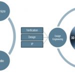
It feels to be at the top of semiconductor technology by having dies with high density of semiconductor design at sub-20nm technology node stacked together into a 3D-IC to form a complete SoC which can accommodate billions of gates. However there are multiple factors to be looked at in order to make that successful amid often conflicting… Read More





Silicon Insurance: Why eFPGA is Cheaper Than a Respin — and Why It Matters in the Intel 18A Era