
SoC designers can code RTL, run logic synthesis, perform place and route, extract the interconnect, then simulate to measure power values. Though this approach is very accurate, it’s also very late in the implementation flow to start thinking about how to actually optimize a design for the lowest power while meeting all… Read More

Author: Daniel Payne
Semiconductor IP and Correct-by-construction Workspaces
SoC hardware designers could learn a thing or two from the world of software development, especially when it comes to the topic of managing complexity. Does that mean that hardware designers should literally use a software development environment, and force fit hardware design into file and class-based software methodologies?… Read More
Special Interest Group for HSPICE at DesignCon in Two Weeks

DesignCon brings together engineers from around the world that are interested in IC design, package design and board design, plus the signal integrity issues of creating high-speed systems. In just two weeks there’s a Special Interest Group(SIG) just for users of HSPICE in their tool flow, and it meets for three hours during… Read More
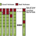
An Update on the OpenPDK for IC Design

IC designers use EDA tools to implement their logical and physical design, and these tools require foundry-specific information for:
- Design Rule Checking (DRC)
- Layout Versus Schematic (LVS)
- Library Symbols
- Parasitic EXtraction (PEX)
Social Media at Aldec

I’ve been blogging about EDA and Semiconductor companies using social media to create new ways to talk and listen to engineers, so today I looked at Aldec and how they are using social media. Aldec offers EDA products for: FPGA Simulation, functional verification, emulation, and MIL/Aero verification. Their Home page … Read More
Mastering the Magic of Multi-Patterning

I’ve been quite impressed that modern ICs use a lithography process with 193nm light sources to resolve final feature sizes at 20nm and smaller dimensions. We’ve been blogging about Double Patterning Technology (DPT) some 45 times in the past few years that enable 20nm fabrication, so one big question for me is, “How… Read More
Early Thermal and Power Simulation Using Virtual Prototyping for Pedestrian Detection Applications

In the 1970’s we designed ICs first and when silicon came back then we measured the power and junction temperature. At that time there were no EDA simulation tools or models for full-chip power and temperature analysis. Fast forward to 2013 and we find that temperature and power are still demanding requirements for MPSoC … Read More
Social Media at Silvaco

Founded back in 1984, Silvaco has been in business for some 29 years now, focusing on the TCAD and EDA markets.
Browsing their Home page at www.silvaco.com we find four social media links in the footer: Facebook, Twitter, YouTube and LinkedIn.… Read More
EDA and Semi IP Stocks in 2013: MENT, ARMH, CDN, SNPS, ANSS, CEVA, IMG.L

2013 was an up year for the stock markets as both the DJIA and the tech-heavy NASDAQ showed significant growth, so how did EDA and Semi IP companies do in the past 12 months? A quick stock plot from Yahoo Finance shows us that only two of the seven companies beat the NASDAQ: ARMH, MENT.… Read More
The Most Popular Blog Posts at Cadence in 2013

I spend about an hour a day reading blogs from EDA companies, foundries, independent bloggers and of course, SemiWiki. Richard Goering at Cadence assembled a top 10 list of the most popular blogs posted on their site in 2013, revealing that engineers were most interested in: FinFETs, 20nm and smaller nodes, memory technology and… Read More


ASML High-NA EUV is Not Ready for High-Volume Production