You are currently viewing SemiWiki as a guest which gives you limited access to the site. To view blog comments and experience other SemiWiki features you must be a registered member. Registration is fast, simple, and absolutely free so please,
join our community today!
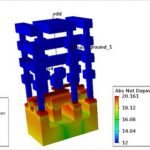
Process and device engineers have a tough task to model and simulate an IC process prior to fabricating silicon, however this approach is much better than the alternative choice in the 1970’s of just running multiple lots of wafers and then making measurements to see if your node was meeting specifications. Out of Stanford… Read More
Spotting trends is an essential insight for marketing folks, general managers and C-level executives in our semiconductor industry. You could read hundreds of press releases, attend dozens of conferences, and interview all of the major thought leaders to help spot an emerging trend, or you could subscribe to a service like IC… Read More
The state of Texas hosted two or our industry’s big technical conferences and trade shows this year: DAC and ITC (International Test Conference). IC designers know about DAC in Austin, and test engineers know about ITC in Dallas. I travelled to Austin to cover DAC this past summer, and I was able to connect with Robert Ruiz … Read More
When I first started doing circuit design with Intel at the transistor level back in the late 1970’s we had exactly two EDA tools at our disposal: an internally developed SPICE circuit simulator, and a commercial IC layout system. Over the years at Intel the internal CAD group added many more automation tools: gate level simulator,… Read More
Several years ago a former EDA co-worker went to work for MathWorks, so I started paying a lot more attention to this privately held company that is well known for the MATLAB language and analysis environment. Engineers at MathWorks have created a graphical environment called Simulink for both simulation and model-based design… Read More
Last Friday I learned something new about IoT by attending a SEMI event in Wilsonville, OR just a few short miles away from where I live in Tualatin. SEMI puts on two events here in Oregon each year, and their latest event on IoT Sensors was quite timely and popular judging by how many attendees showed up. First up was Jeff Miller from … Read More
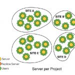
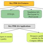
In our semiconductor ecosystem we have foundries on one side supplying all of that amazing silicon technology, and IC designers on the other side that take their system ideas then go implement them in a SoC using a specific foundry. The required interface between foundry and chip designers has been the Process Design Kit (PDK), … Read More
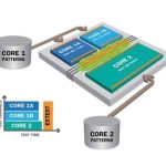
In the early days of IC design there were arguments against using any extra transistors or gates for testability purposes, because that would be adding extra silicon area which in turn would drive up the costs of the chip and product. Today we are older and wiser, realizing that there are product pricing benefits to quickly test each… Read More
I’ve been following Cadence Design Systems ever since it was formed in 1988 by the merger of SDA Systems and ECAD, Inc. At that time I was working at Silicon Compiler Systems, soon to be acquired by Mentor Graphics. ClioSoft is another company that I’ve known about for several years now, mostly for their design management… Read More
From a consumer viewpoint I want the longest battery life from my electronic devices: iPad tablet, Galaxy Note 4 smart phone, Garmin Edge 820 bike computer, and Amazon Kindle book reader. In September I blogged about RTL Design Restructuring and how it could help achieve lower power, and this month I’m looking forward to … Read More


Captain America: Can Elon Musk Save America’s Chip Manufacturing Industry?