You are currently viewing SemiWiki as a guest which gives you limited access to the site. To view blog comments and experience other SemiWiki features you must be a registered member. Registration is fast, simple, and absolutely free so please,
join our community today!
I’ve been visiting DAC for decades now, at first as an EDA vendor and since 2004 as a freelance EDA consultant. There’s always a buzz about what’s new, semiconductor industry trends, who is getting acquired and the latest commercial EDA and IP offerings. There’s so much vying for my attention at DAC each… Read More
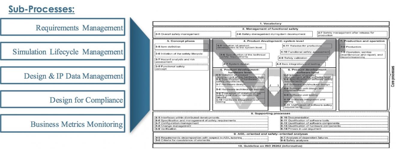
Reading the many articles on SemiWiki and other publications we find experts talking about the automotive market, mostly because it’s in growth mode, has large volumes and vehicles consume more semiconductors every year. OK, that’s on the plus side, but what about functional safety for automotive electronics?… Read More
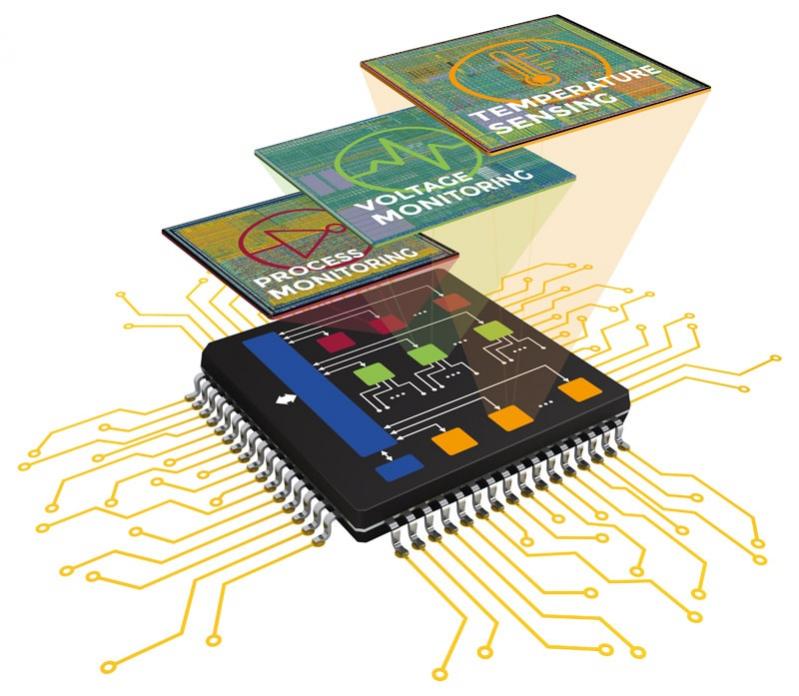
Have you ever wondered how process variation, thermal self-heating and Vdd levels affect the timing and yield of your SoC design? If you’re clock specification calls for 3GHz, while your silicon is only yielding at 2.4GHz, then you have a big problem on your hands. Such are the concerns of many modern day chip designers. To… Read More
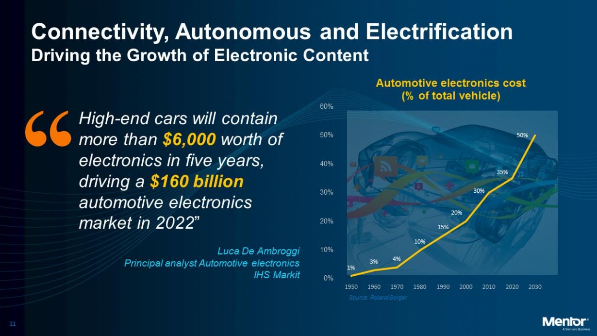
Most of us continue to drive cars and for me there’s always been a fascination with all things electrical that go into the actual design of a car. I’ve done typical maintenance tasks on my cars over the years like changing the battery, installing a new radio, replacing bulbs, changing a fuse, swapping out dashboard lights,… Read More
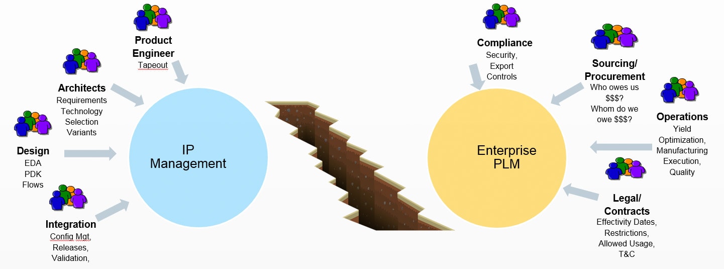
No single EDA company provides all of the tools needed to define requirements, design exploration, track IP, simulate, manage and verify a complex SoC system, so it makes sense that EDA vendors and point tool companies have tools that work together to achieve all of these difficult tasks. Systems design has been around for decades… Read More
Computer vision as a research topic has been around since the 1960’s and we are enjoying the benefits of this work in modern-day products all around us as robots with computer vision are performing an increasing number of tasks, even our farmers are using computer vision systems to become more productive:
…
Read More
In the old days to learn about new semiconductor IP you would have to schedule a sales call, listen to the pitch, then decide if the IP was promising or not. Today we have webinars which offer a lot less drama than a sales call, plus you get to ask your questions by typing away at the comfort of your desk, hopefully wearing headphones as … Read More
On LinkedIn I have some 2,116 connections and many of those are students looking to enter the field of EDA, IP or semiconductor design. What a wonderful opportunity these students have by attending the 55th annual DAC in San Francisco this summer from June 24-28. Technical sessions, keynote speeches, exhibitors, networking, … Read More
I remember meeting John Durbetaki at Intel where we both worked in 1980, it was an exciting time and something called the Personal Computer had just been introduced by companies like Commodore, Apple and Radio Shack (yes, Radio Shack). IBM was rather late to the party with their PC in 1981, however when IBM entered the market then … Read More
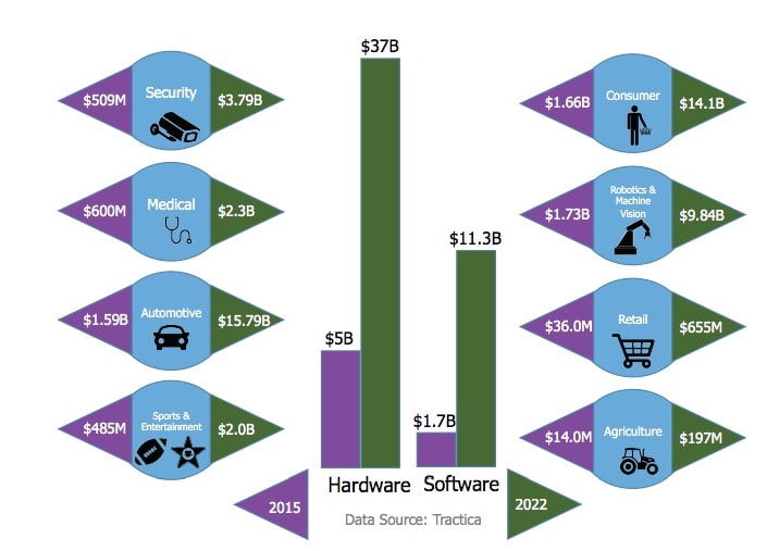
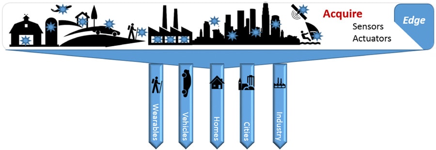
The IoT market opportunities in segments like wearables, vehicles, home, cities and industrial are all growing thanks to the combination of semiconductors, sensors, software and systems technology. New hardware designs for IoT edge devices appear on a daily basis, and the companies behind these new products can often be start-ups… Read More


Captain America: Can Elon Musk Save America’s Chip Manufacturing Industry?