You are currently viewing SemiWiki as a guest which gives you limited access to the site. To view blog comments and experience other SemiWiki features you must be a registered member. Registration is fast, simple, and absolutely free so please,
join our community today!
I’ve been following Solido as a start-up EDA vendor since 2005, then they were acquired by Siemens in 2017. At the recent User2User event there was a presentation by Kwonchil Kang, of Samsung Electronics on the topic, ML-enabled Statistical Circuit Verification Methodology using Solido. For high reliability circuits… Read More
It was back in 1991 that Cadence first announced the Virtuoso product name, and here we are 32 years later and the product is alive and doing quite well. Steven Lewis from Cadence gave me an update on something new that they call Virtuoso Studio, and it’s all about custom IC design for the real world. In those 32 years we’ve… Read More
Generative AI is all the rage with systems like ChatGPT, Google Bard and DALL-E being introduced with great fanfare in the past year. The EDA industry has also been keen to adopt the trends of using AI techniques to assist IC engineers across many disciplines. Saugat Sen, Product Marketing at Cadence did a video call with me to explain… Read More
Traveling by car is something that I take for granted and I just expect that my trips will be safe, yet our cars are increasingly using dozens of ECUs, SoCs and millions of lines of software code that combined together present a target for hackers or system failures. The Automotive Safety Integrity Levels (ASIL) are known by the letters:… Read More
The Systems Modeling Language (SysML) is used by systems engineers that want to specify, analyze, design, verify and validate a specific system. SysML started out as an open-source project, and it’s a subset of the Unified Modeling Language (UML). Mirabilis Design has a tool called VisualSim Architect that imports your… Read More
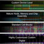
My IC design career started out with DRAM design back in 1978, so I’ve kept an eye on the developments in this area of memory design to note the design challenges, process updates and innovations along the way. Synopsys hosted a memory technology symposium in November 2022, and I had a chance to watch a presentation from SK hynix… Read More
Analog IC designers can spend way too much time and effort re-using old, familiar, manual iteration methods for circuit design, just because that’s the way it’s always been done. Circuit optimization is an EDA approach that can automatically size all the transistors in a cell, by running SPICE simulations across… Read More
Earlier I blogged about IC and ASIC functional verification, so today it’s time to round that out with the state of FPGA functional verification. The Wilson Research Group has been compiling an FPGA report every two years since 2018, so this marks the third time they’ve focused on this design segment. At $5.8 billion… Read More
A quick Google search for “2.5D 3D IC” returns 669,000 results, so it’s a popular topic for the semiconductor industry, and there are plenty of decisions to make, like whether to use an organic substrate or silicon interposer for interconnect of heterogenous semiconductor die. Design teams using 2.5D and … Read More
Way back in 2002 there was a study from Collett International Research on functional verification, and since 2010 the Wilson Research Group has continued that same kind of study with a new report every two years. What attracts me to this report is that it doesn’t just look at the installed base of one EDA vendor, instead it looks… Read More


Captain America: Can Elon Musk Save America’s Chip Manufacturing Industry?