You are currently viewing SemiWiki as a guest which gives you limited access to the site. To view blog comments and experience other SemiWiki features you must be a registered member. Registration is fast, simple, and absolutely free so please,
join our community today!
During my trip through Asia last week I attended the Taiwan ESD Workshop. Hsinchu is densely populated with some of the smartest semiconductor people in the world so it is well worth the trip, absolutely. As it turns out ESD is one of the top concerns in semiconductor design and manufacture. The current rule based and simulation … Read More
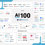
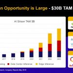
I came across a report on the 100 most promising AI start-ups. The report claimed that CBInsights had “selected the 100 most promising AI start-ups from a pool of 3K+ companies based on several factors …” Wait, what … 3K+ companies!?!? This was a stunning reminder of the sheer magnitude of what is shaping up to be a veritable tsunami… Read More
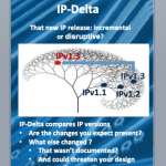
The rising complexity of modern SoC designs, as enabled by progressing manufacturing technology, leads to an increasing validation challenge as the only way to manage complexity increase is by re-using more pre-designed IP blocks. These IP-blocks are provided by various suppliers such as a foundry partner, internal design… Read More
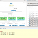
Portable stimulus has been a hot topic for a couple of years in the EDA and semiconductor industries. Many observers see this approach as the next major advance in verification beyond the Universal Verification Methodology (UVM), and the next step higher in abstraction for specifying verification intent. The basic idea is to … Read More
Naveed Sherwani, President and CEO of SiFive, did the keynote for this year’s Silicon Summit. This is one of the premier events for the C level executives in Silicon Valley, absolutely. Naveed is one of the top visionaries for the semiconductor industry and he certainly did not disappoint this time or any other time in my experience.… Read More
SEMICON West and ES Design West are right around the corner here in San Francisco and I wanted to point out the Meet the Experts segment in the appropriately named Meet the Experts Theater. Great idea really and a super great line-up. The best part of course is actually meeting the experts. Over my 35 year semiconductor career I have… Read More
During my Taiwan visit, prior to Las Vegas, I was fortunate to spend time with Willy Chen and Vivian Jiang to prepare for the cloud panel I moderated at #56thDAC. Willy and Vivian are part of the ever-important Design Infrastructure Marketing Division of TSMC, which includes the internal and external cloud efforts. TSMC first announced… Read More
One of the perks of blogging on SemiWiki is the events you get to attend for FREE and the amazing people you get to meet and Wally Rhines is certainly one of those people. You will not find a more intelligent, innovative, and genuinely nice group of people in my experience. Having traveled the world meeting thousands of people I can tell… Read More
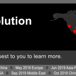
Join SiFive Tech Symposiums in Tokyo, Daejeon, Pangyo, Hsinchu, Singapore and Sydney
As we make our way around the world meeting and engaging with others in the semiconductor and hardware design community, we are seeing an increased interest in RISC-V based hardware innovation. This is due in large part to the emergence of market-ready… Read More
As much as I love all EDA vendors I must say Cadence did the best DAC this year. Great booth, great location, excellent content, and of course a great party. The 5G presentation in the Cadence booth by Ian Dennison was of great interest to me as I am still trying to wrap my head around this whole 5G thing. I was able to meet with Ian privately… Read More


Podcast EP357: How Gonka is Changing the Way AI is Accessed with David Liberman