AI’s rapid expansion is reshaping semiconductor design. The compute and I/O needs of modern AI workloads have outgrown what traditional SoC scaling can deliver. As monolithic dies approach reticle limits, yields drop and costs rise, while analog and I/O circuits gain little from moving to advanced process nodes. To sustain performance growth, the industry is turning to chiplets—modular, scalable building blocks for multi-die designs that redefine how high-performance systems are built.
Why Chiplets Matter
Forecast to become a $411 billion market by 2035 (IDTechEx), multi-die designs divide large SoC functions into smaller, reusable dies (also called chiplets) that can be integrated into a single system-in-package (SiP). These chiplets may be heterogeneous or homogeneous, replicating cores for scaling. SiPs can rely on standard organic substrates or advanced interposers that enable dense interconnects and greater functionality within a compact footprint.
The vision is an open marketplace where designers can mix and match chiplets from multiple suppliers. Beyond JEDEC’s HBM memory modules, however, widespread adoption of off the shelf chiplets has been limited by fragmented standards and fragmented use cases. Progress continues with UCIe (Universal Chiplet Interconnect Express), Arm’s Chiplet System Architecture (CSA), and new industry collaborations aimed at breaking these barriers.
System Partitioning and Process Node Choices
The first step in chiplet design is deciding how to partition system functions. Compute, I/O, and memory blocks can each be implemented on the process node that offers the best balance of power, performance, and cost. For example, an AI compute die benefits from the latest node, while SRAM or analog functions may be built on less advanced—and less expensive—nodes.
Latency and bandwidth demands guide how these blocks connect. A 2.5D interposer may provide sufficient performance, but latency-sensitive systems sometimes require 3D stacking, as seen in AMD’s Ryzen 7000X3D processors, where compute and cache are vertically integrated for faster data access.
Designing Die-to-Die Connectivity
Interconnect performance defines chiplet success. UCIe has become the industry’s preferred die-to-die standard, offering configurations for both cost-efficient organic substrates and high-density silicon interposers. Designers must weigh data rates, lane counts, and bump pitch to achieve the right mix of bandwidth, area, and power.
AI I/O chiplets, for instance, may require UCIe links supporting 16G–64G data rates to maintain low-latency communication with compute dies. Physical layout choices for interface IPs—single-row or double-stacked PHYs—may affect the beachfront area available for die-to-die interfaces and affect both area efficiency and design complexity.
Bridging UCIe’s streaming interface with on-chip protocols such as AXI, Arm CXS, or PXS is also key to maximizing throughput and minimizing wasted bandwidth.
Advanced Packaging and Integration
Packaging now sits at the heart of semiconductor innovation. Designers must choose between lower-cost organic substrates and denser 2.5D or 3D approaches. Silicon interposers deliver unmatched interconnect density but come with size and cost constraints. Emerging RDL (Redistribution Layer) interposers provide a balanced alternative—supporting larger system integration at reduced cost. Typical bump pitches range from 110–150 microns for substrates to 25–55 microns for interposers, shrinking further for 3D stacks.
Thermal, mechanical, and power-integrity challenges grow as multiple chiplets share one package. Early co-design across silicon and packaging domains is essential. Testability must also be planned in advance, using the IEEE 1838 protocol and multi-chiplet test strategies to ensure known-good-die (KGD) quality before assembly.
Securing and Verifying Multi-Die Designs
With multiple chiplets, the attack surface widens. Each chiplet must be authenticated and protected through attestation and secure boot mechanisms. Depending on the application, designers may integrate a root of trust to manage encryption keys or isolate sensitive workloads.
Data in transit must be secured using standards such as PCIe and CXL Integrity and Data Encryption (IDE), DDR inline memory encryption (IME), or Ethernet MACsec. Verification is equally critical: full-system simulation, emulation, and prototyping are required to validate die interactions before fabrication. Virtual development environments enable parallel software bring-up, shortening time-to-market.
Synopsys and Arm: Simplifying AI Chip Design
AI accelerators bring these challenges into sharp focus. They demand enormous compute density, massive bandwidth, and efficient integration across heterogeneous dies. To address this complexity, Synopsys and Arm—long-time collaborators—are combining their expertise to streamline AI and multi-die development.

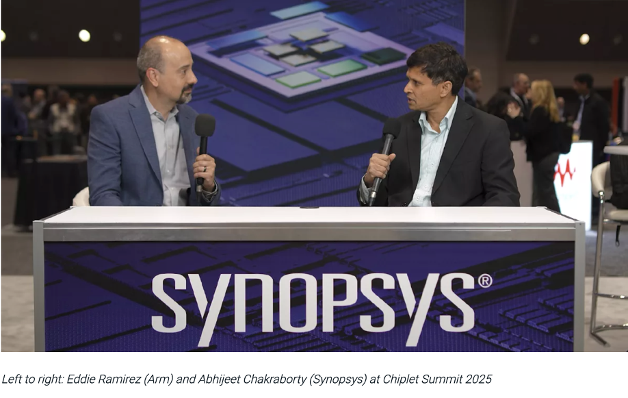
At Chiplet Summit 2025, Synopsys VP of Engineering Abhijeet Chakraborty and Arm VP of Marketing Eddie Ramirez discussed how their companies are reducing design risk and speeding delivery. Under Arm Total Design, Arm’s Neoverse Compute Subsystems (CSS) are now pre-validated with Synopsys IP, while Synopsys has expanded its Virtualizer prototyping solution and Fusion Compiler quick-start flows for the Arm ecosystem. These integrations let customers implement Arm compute cores more efficiently, validate designs earlier, and begin software development long before silicon arrives.
“We feel we are barely scratching the surface,” Chakraborty noted. “There’s a lot more work we can do in this space.” Both leaders emphasized that interoperability, reliability, and security will remain top priorities as chiplet ecosystems evolve.
The Road Ahead
The semiconductor industry is shifting from monolithic to modular design. Continued progress will depend on collaboration, standardization, and shared innovation across companies and ecosystems. With Synopsys advancing chiplet standards, design flows, and verified IP subsystems, the path from concept to production is becoming faster and more predictable. Customers can focus on their core competencies, while offloading other aspects of the design to respective experts in those areas for fast and reliable time-to-market.
The next generation of AI systems won’t rely on bigger chips—they’ll be built from smarter, interconnected chiplets, delivering scalable performance, efficiency, and flexibility for the most demanding compute workloads of the future.
Also Read:
The Rise, Fall, and Rebirth of In-Circuit Emulation: Real-World Case Studies (Part 2 of 2)
Statically Verifying RTL Connectivity with Synopsys
Why Choose PCIe 5.0 for Power, Performance and Bandwidth at the Edge?
Share this post via:


Comments
There are no comments yet.
You must register or log in to view/post comments.