Heterogeneous multi-die integration is gaining more momentum all the time. The limited roadmap offered by Moore’s Law monolithic, single-die integration has opened the door to a new era of more-than-Moore heterogeneous integration. The prospects offered by this new design paradigm are exciting and the entire ecosystem is jumping in to bring it all closer to reality. Standards to help make chiplets more widely available, new materials to increase density and a host of design technologies to make it all work are underway. While all this promises to deliver an integrated design capability, the elephant in the room is where to start. High quality and well-integrated up-front planning at the system level is a necessity to ensure success for the next wave of designs. Siemens Digital Industries Software recently announced a comprehensive new approach to 3D IC design. They seem have gotten it right regarding how to scope the problem for success. Let’s examine how Siemens provides a complete 3D IC solution with Innovator3D IC.
What Problem Needs Solving?

I recently had the opportunity to chat with Keith Felton, product marketing manager at Siemens for High-Density Advanced Packaging (HDAP) solutions. Keith has a long history of solving advanced design and packaging challenges.
Keith explained that there is indeed a lot of work going on to address the challenges of tasks such as place and route for multi-die heterogeneous designs. All of that is quite important, but Keith pointed out that early feasibility planning and analysis of the system, before implementation begins is a critical step that needs to be addressed first. The questions that must be answered before implementation begins include:
- What are the system thermal considerations?
- Can I get the right level of power to all parts of the system?
- How will the substrate and the overall package behave under typical and extreme operation?
This is just a summary of a much longer list of questions that must be addressed early in the design flow and at the system level. This is really the only way to avoid downstream re-work that can have substantial negative impact. Keith explained that part of the innovation here is to build a digital twin model of the system early. Using this model a design cockpit can be created that allows forward visibility to all downstream tools to allow tradeoffs to be assessed and roadblocks avoided before detailed implementation begins.
This made perfect sense to me. Let’s look at some of the details of the announcement.
How Siemens Provides a Complete 3D IC Solution with Innovator3D IC
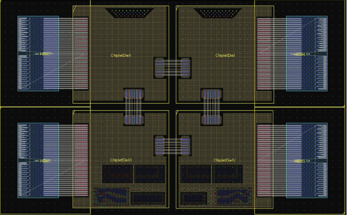
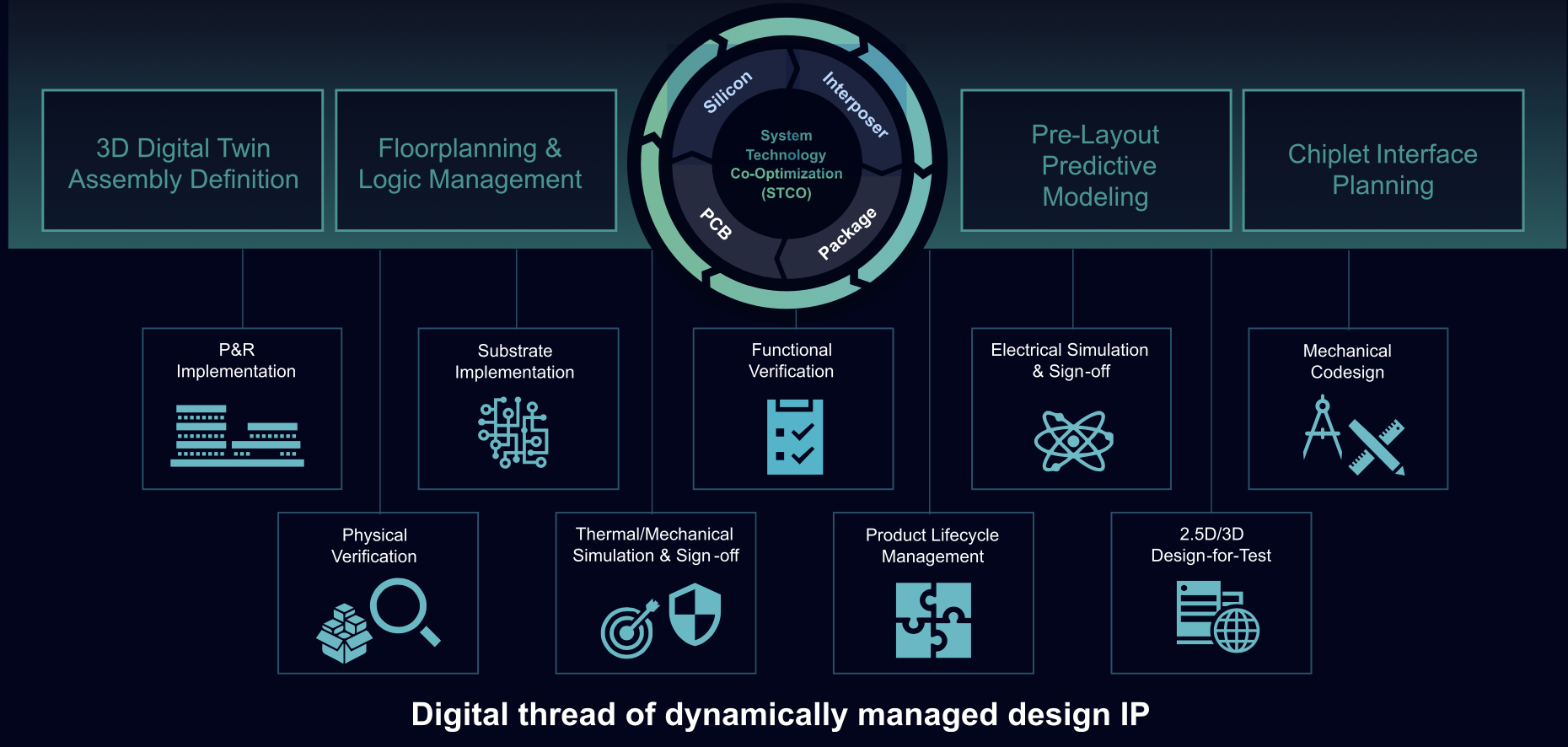
Innovator3D IC delivers the fastest and most predictable path for planning and heterogeneous integration of ASICs and chiplets using the latest semiconductor packaging 2.5D and 3D technology platforms and substrates. The technology provides a unified cockpit for design planning, prototyping and predictive multi-physics analysis. This cockpit constructs a power, performance, area (PPA) and cost optimized digital twin of the complete semiconductor package assembly that in turn drives implementation, multi-physics analysis, mechanical design, test, signoff, and release to fabrication and manufacturing through a managed and secure design IP digital thread conduit.
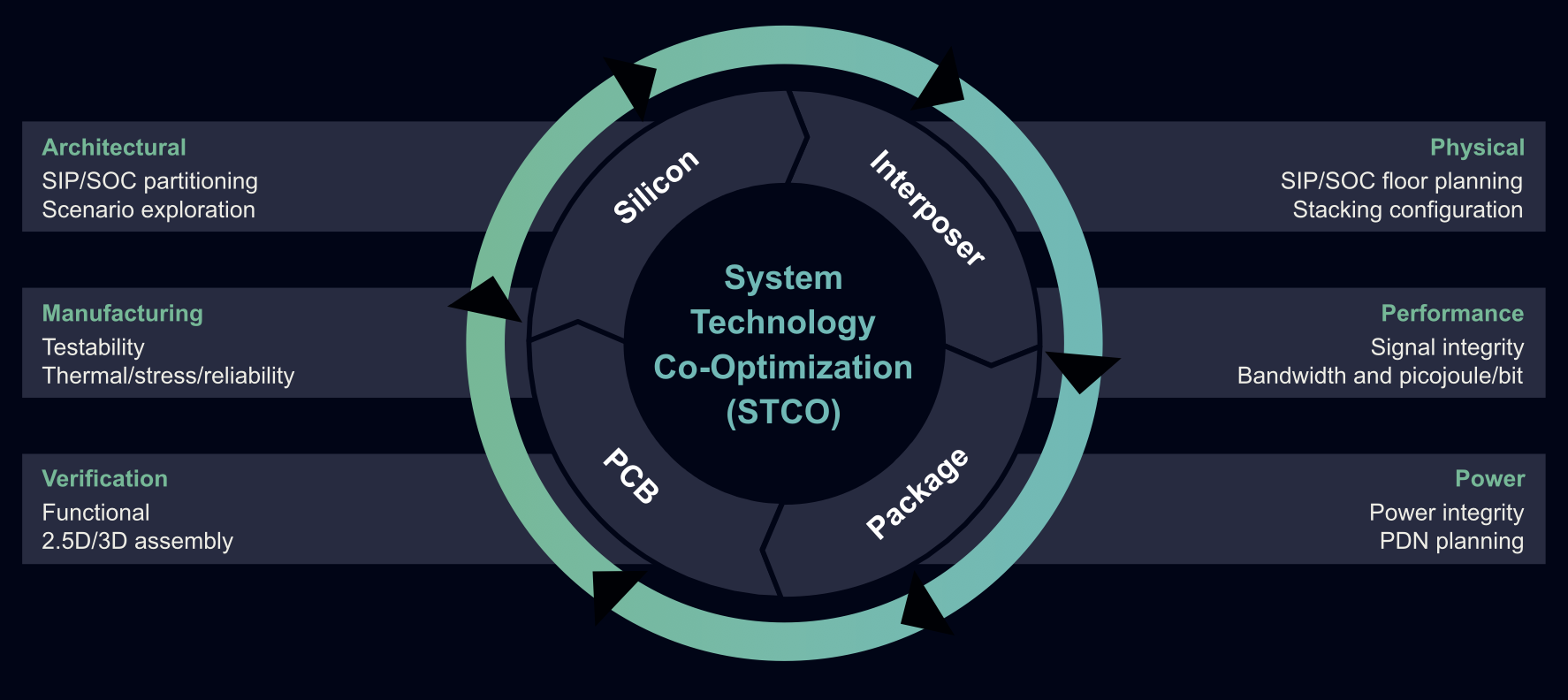
Innovator3D IC is architected around the system technology co-optimization (STCO) methodology process developed by IMEC. STCO is utilized throughout prototyping and planning, design, sign-off, and manufacturing hand-off, concluding with comprehensive verification and reliability assessment.
The figure below summarizes the broad set of capabilities delivered by Innovator3D IC.

Although the cockpit is directly integrated with the extensive Siemens Xcelerator technology portfolio, it supports the integration of third-party point solutions, recognizing that customers may have third party tools in their current design flows that they wish to continue using. The co-optimization employed by Innovator3D IC also makes extensive use of AI technology for co-optimization as shown in the figure below.

Industry standards support is also an important part of the overall solution. A key area is the commitment and support for the growing 3Dblox™ standard that enables EDA tool interoperability, bringing the benefits of improved productivity and efficiency to end users and customers in 3D IC system level designs.
It is also important to ensure frictionless adoption and consumption of existing and new die-to-die interface IP, such as UCIe and BoW. The Open Compute Project Chiplet Design Exchange Working Group (OCP CDX) has enabled direct consumption of standardized chiplet models that will be provided by the emerging commercial chiplet ecosystem.
Predictive multiphysics analysis is also an important part of the solution. During prototyping and planning it is critical to evaluate the performance of all design scenarios before committing to implementation. Innovator3D IC integrates directly with power, signal, thermal, and mechanical stress analyses so that a design scenario can be evaluated quickly, and any issues explored and resolved prior to detailed design implementation. This shift-left approach prevents costly and time-consuming downstream rework and sub-optimal results.
To Learn More
According to the announcement, Innovator3D IC is expected to be available later in 2024. You can learn more about Siemens’ Innovator3D IC software here. You’ll find a lot of useful information there, including a very informative brochure. You can read the complete press release here. And that’s how Siemens provides a complete 3D IC solution with Innovator3D IC.
Share this post via:


Comments
There are no comments yet.
You must register or log in to view/post comments.